Abstract: Interleaved multiphase converters or synchronous buck converters are usually employed to supply power to microprocessors. However, these designs typically have large ripple currents in their inductors, and thus the converters will have relatively high switching losses. One alternative that reduces switching losses is to use a coupled-choke topology in the multiphase converter. The coupled chokes improve supply efficiency by reducing the phase ripple without increasing the output ripple voltage. Furthermore, the combination of the coupled-choke topology and a lower leakage inductance will also improve the converter's transient response.
A similar article appeared in the May, 2009, edition of Power Electronics Technology magazine.
Introduction
Power supplies for today's high-performance microprocessors require high-current, low-voltage DC-DC converters with fast transient responses. Those supplies must deliver currents of more than 100A at voltages of 1V and below. Additionally, they must respond to load-current changes in nanoseconds. During the load changes, moreover, the supply's output voltage must remain within a narrow regulation boundary. However, a small amount of output-voltage "droop" is permitted such that the output voltage decreases slightly within the regulation boundary when the load current increases.
Synchronous buck converters are normally used to power microprocessors. These converters typically step down a 12V input from a bus converter to 1.0V or lower. However, buck converters require higher steady-state levels and a fast transient response to load changes. To achieve that performance, a small inductor allows quick current ramping and can reduce the size of the output capacitor. There is, however, a problem with this approach: small inductor values lead to large ripple current in the inductor and higher switching losses for the converter.
Interleaved multiphase converters substantially cancel the ripple current in the output capacitor. That allows designers to reduce the output capacitor's capacitance without affecting the ripple voltage. Alternatively, they can reduce the inductance per phase so that the power supply responds to load-current changes quicker. There is, nonetheless, still a problem with this design. As the inductance per phase in the uncoupled multiphase buck converter is reduced, phase ripple current increases. So again, the switching losses and the copper losses also increase.
An alternative approach uses a coupled-choke topology in a multiphase converter. This design prevents any increase in switching losses by reducing the phase ripple for the same output-ripple voltage. Additionally, if you use a coupled choke with lower leakage inductance, the converter's transient response can also be improved.
The Coupled-Choke Topology
There are many industry-standard multiphase buck controllers and converters available today. This article uses the MAX8686 controller to compare the performance of a coupled-choke vs. an uncoupled-choke topology in a multiphase converter. Two MAX8686 controllers will be used to form a two-phase buck converter.
The MAX8686 is a current-mode, synchronous PWM step-down regulator with integrated MOSFETs. The controller operates from a 4.5V to 20V input supply, and provides an adjustable output voltage from 0.7V to 5.5V while delivering up to 25A per phase. The controller can be configured for single-phase as well as multiphase operation. For multiphase operation, the MAX8686 can operate in master or slave mode.
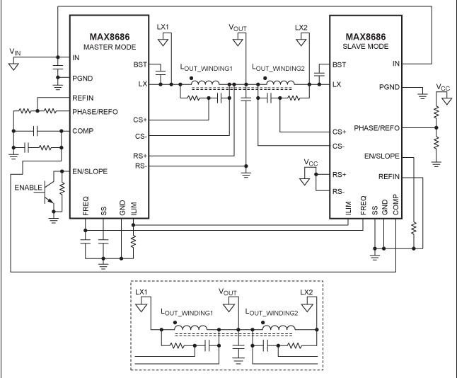
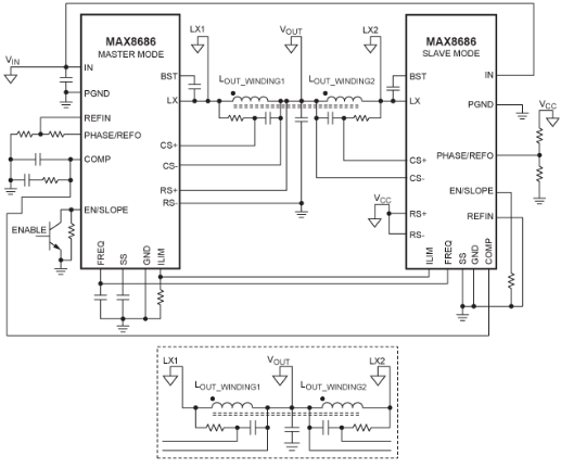
Figure 1 illustrates the two approaches: two-phase converters with coupled-choke and uncoupled-choke topologies. LOUT_WINDING1 and LOUT_WINDING2 can be two windings of the coupled choke or two physically separate inductors. With coupled chokes, how the two windings are connected (i.e., in phase or out of phase) is very important.
A prototype board using the MAX8686 is shown in Figure 2. The converter is running at 400kHz; the input voltage is 12V and output voltage is 1.2V with a maximum-rated current of 50A. This converter delivers up to 40A at +70°C with as little as 200 LFM of airflow.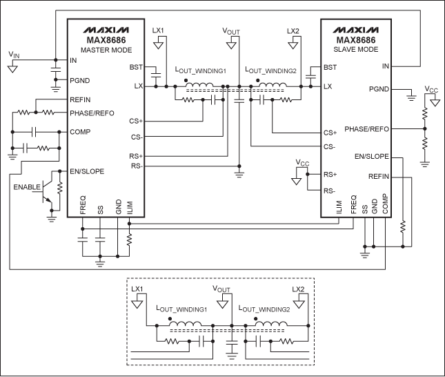
Figure 1. Schematic of a two-phase buck converter with a coupled choke. Note the polarity of winding for out-of-phase connection. The winding polarity shown here produces the best performance. In the inset, two inductors are also used to reduce the magnetic coupling. Now polarity does not matter.
Figure 2. A prototype board with two MAX8686 PWM controllers and a coupled choke can deliver a maximum current of 50A at an output voltage of 1.2V.
Issues Involving the Inductors
Inductor current waveforms and LX voltage waveforms using two inductors are shown in Figure 3. The two inductors are Vishay? model 0.56μH-IHLP-4040DZ-11.
Inductor currents are combined in the output capacitors. Figures 3b and 3c show the same waveforms for the converter using a coupled choke with two windings. The coupled choke used for this example is the BI Technologies HM00-07559LFTR which has a self-inductance of 0.6μH (typ) and leakage inductance of 0.3μH (min). The waveform in Figure 3b shows inductor current when coupled-choke windings are connected out of phase. Figure 3c shows current waveforms when windings are connected in phase. The in-phase connection is not recommended because it increases the phase current, making the converter less efficient.
Figure 3a shows that with two separate inductors there is only one current pulse per phase through each inductor. This compares with Figures 3b and 3c, where there are two current pulses per switching cycle with the coupled choke. However, the in-phase connection of the winding causes current to decrease rather than increase when the second phase turns on. When the windings are connected out of phase with the coupled-choke approach, the ripple current is cancelled. It does not matter how the two separate inductors are connected, as there is no mutual inductance between them. The waveform in Figure 3d shows phase current with a coupled choke and with the windings connected out of phase at a load current of 40A.
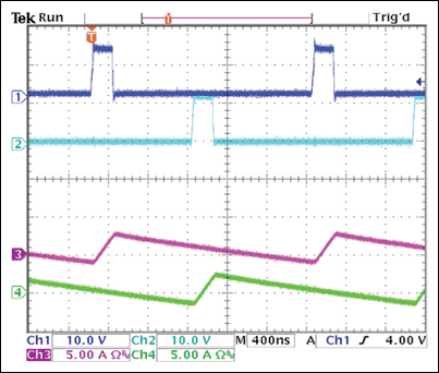 Figure 3a Two-phase board with two chokes. Ch1: master LX voltage; Ch2: slave LX voltage; Ch3: master inductor current; Ch4: slave inductor current; VIN = 12V; VOUT = 1.2V/no load. |
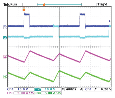 Figure 3b Two-phase board with coupled choke, out of phase. Ch1: master LX voltage; Ch2: slave LX voltage; Ch3: master inductor current; Ch4: slave inductor current; VIN = 12V; VOUT = 1.2V/no load. |
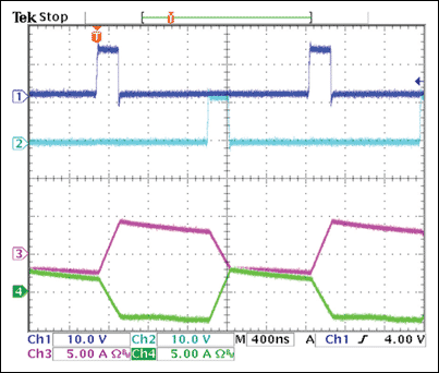 Figure 3c Two-phase board with coupled choke, in phase. Ch1: master LX voltage; Ch2: slave LX voltage; Ch3: master inductor current; Ch4: slave inductor current; VIN = 12V; VOUT = 1.2V/no load. |
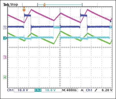 Figure 3d Two-phase board with coupled choke, out of phase. Ch1: master LX voltage; Ch2: slave LX voltage; Ch3: master inductor current; Ch4: slave inductor current; VIN = 12V; VOUT = 1.2V/40A. |
The selection of the output inductor is very important for efficiency and transient response optimization. Its value is calculated based on the amount of permitted inductor ripple current. A larger inductance can reduce ripple current and increase efficiency, provided that the DC resistance of the choke is not increased. However, the larger inductance value will increase the inductor's size since a larger value will require more wire. However, to keep the resistance value constant, a larger diameter wire must be used, thus making the inductor larger.
If a larger value inductor is used, the output inductor's current slew rate will slow down during a load transient. LIR is defined as the ratio of ripple current to load current per phase. A compromised LIR value ranges from 0.2 to 0.5. LIR can be higher when more phases are used to take advantage of ripple-current cancellation. Therefore, to ensure optimal LIR the selected inductor should have a low DC resistance and the saturation current should be greater than the peak inductor current. If the inductor's DC resistance is used to sense output current, then the current-sense signal should have enough amplitude for current-mode operation of the MAX8686. A signal level of 10mV (min) is recommended to avoid any sensitivity to noise.
Issues Involving the Capacitors
An input capacitor is used both to reduce the peak current drawn from the DC input source, and to reduce noise and ripple voltage caused by the circuit switching. The input capacitor must meet the ripple-current requirement imposed by the switching current. Low-ESR (equivalent series resistance) aluminum electrolytic, polymer, or ceramic capacitors should be used to avoid large-voltage transients at the input during a large-step load change at the output. The ripple-current specifications provided by the manufacturer should be carefully reviewed for temperature derating. A 10°C to 20 °C rise in temperature is acceptable. Additional small-value low-ESL (equivalent series inductance) ceramic capacitors can be used in parallel to reduce any high-frequency ringing.
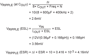
The key selection parameters for output capacitors are the actual capacitance value, the ESR, ESL, and the voltage rating requirement. These parameters affect overall stability, output voltage ripple, and transient response. The output ripple voltage has three components: variations in the charge stored in the output capacitor, the voltage drop across ESR, and ESL due to current flowing into and out of the capacitors. The design equations used to select the capacitors are given below.
Design Calculations
Starting Conditions
VIN 12V; VOUT = 1.2V; IOUT = 50A; η = 0.85
Operating frequency = 400kHz; N = 2
N = number of phases; η = efficiency factor
Inductor Value Calculations
Start by calculating the power dissipation and the input current for the converter:
POUT = VOUT × IOUT
PIN = POUT/η
PDISS = PIN - POUT
60W = 1.2V × 50A
70.58W = 60W/0.85
Therefore:
PDISS = 10.58W(70.58W - 60W)
IIN(av) = PIN/VIN = 70.58W/12V = 5.882A
Next, calculate the output inductor value:
LIR = inductor ripple current factor = IΔ/IOUT = 0.2
Now solve for ΔI  0.2 × IOUT (This will be needed in the output ripple calculation.)
The closest off-the-self inductor value is 0.56μH and it has a DC resistance of 0.0017Ω.
Peak Current Calculations
Input Capacitor (CIN) Calculation
N × D = 0.235, and for N × D < 1
Where IIN(RMS) is the RMS ripple current through the input capacitor.
Output Ripple Voltage (VRIPPLE) Calculations
Assume:
ESR = (2.5/6) × 10-3 (ESR of output capacitor)
ESL = (1/6) × 10-9 (ESL minus the parasitic inductance of output capacitor)
COUT = 600μF
Calculate VRIPPLE:
Thus, the full VRIPPLE voltage is:
VRIPPLE (COUT) + VRIPPLE (ESL) + VRIPPLE (ESR)
Therefore:
VRIPPLE = approximately 10mV
Performance Improvements of the Coupled-Choke Topology
Figures 4a and 4b show the transient load comparison for the converters with coupled choke and two separate inductors. The coupled-choke approach delivers a considerably improved transient response because the transient load in the coupled choke is restricted by leakage inductance only, and not by self-inductance. This design experienced no decrease in phase inductance.
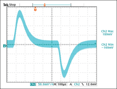 Figure 4a Two-phase board with two separate inductors. Transient loading; Ch1: O/P voltage; VIN = 12V; VOUT = 1.2V/5A–25A–5A. |
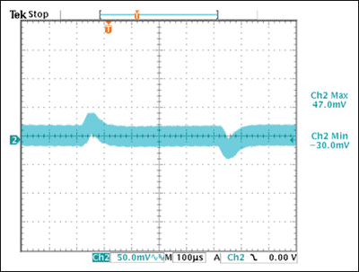 Figure 4b Two-phase board with coupled choke, out of phase. Transient loading; Ch1: O/P voltage; VIN = 12V; VOUT = 1.2V/5A–25A–5A. |
The waveforms in Figure 5a and 5b show the output ripple voltage at full load using both approaches. The curves in Figure 6 compare the efficiency for an uncoupled and coupled version of two-phase converters. Once again, efficiency is also improved with the coupled choke. No-load current will be more with the coupled choke, which is why the coupled-choke approach will have a lower efficiency during light load conditions. At higher loads the coupled-choke topology delivers better efficiency.
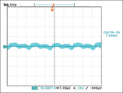 Figure 5a |
Figure 5b |
Figure 6. The converter efficiency for the coupled inductor is better for heavy loads. For light loads the two separate inductors deliver slightly better efficiency.
 電子發燒友App










評論