Trends in High-Performance Power-Supply Design for Automotive Infotainment
Abstract: This article provides a practical framework for selecting and optimizing power-supply architectures for automotive infotainment electronics. First, a summary of design constraints and application requirements is provided. Then, the most popular power-supply architectures are discussed within the context of the application requirements. Finally, a selection of Maxim automotive power-management ICs (PMICs) is presented as building blocks of the power-supply architectures explored in the article.
DS1875 Introduction
More than half of the 2012 model year cars in the EU, Japan, and U.S. will feature a color screen, a navigation system, satellite radio, or some other form of in-car infotainment. Consequently, the automotive power supplies in year 2012 will look significantly different than their predecessors a decade earlier.
The conflicting expectations of high reliability, lower cost, and faster design cycles have forced power-supply designers to adopt techniques not previously used in a typical automotive power supply.
Five Common Constraints of Power-Supply Design for Automotive
Most automotive power-supply architectures are shaped by six generic constraints:
- VIN Range: The voltage transient range on a 12V battery powerline determines the input voltage range of converter ICs.
A typical car battery operates in the 9V to 16V range. The nominal voltage of a healthy battery is 12V when the engine is off, and around 14.4V when the engine is on. This range, however, easily extends to ±100V when the transient conditions are involved. For the full specification of these transients, please refer to the ISO7637-1 industry standard. Figures 1 and 2 are part of this ISO7637 standard and outline the most critical conditions that need to be addressed by a high-voltage converter in an automotive power supply. Besides the ISO7637-1, there are new transient conditions defined for battery-operated or environmentally friendly gas engines. Most of the new specifications are driven by individual OEMs and do not necessarily follow an industry standard. Nonetheless, overvoltage and undervoltage protection are required for all new systems.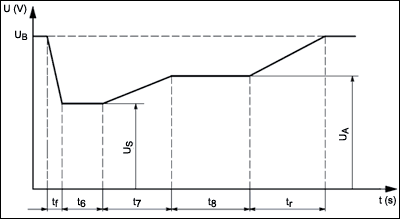
Figure 1. A cold crank profile.
Figure 2. A load dump profile.
- Heat Budget: The heat-dissipation budget sets the minimum DC-DC conversion efficiency requirement.
Applications with little or no airflow tend to get hot (> 85°C) quickly, if there is a heat source (> 1W) in the casing and the ambient temperature is high (> 30°C). Most audio amplifiers, for example, must be placed on heatsinks with sufficient airflow because of high heat dissipation. Also, the PCB material and amount of copper on a specific area of the board effects the converter's maximum heat-dissipation capability. Without heatsink, maximum heat dissipation over an exposed pad of a package is typically limited to 2W to 3W at 85°C. As ambient temperature increases, the heat dissipation capability decreases significantly.
For a typical car battery-to-low-voltage (e.g., 3.3V) conversion, linear converters lose 75% of the input power to heat due to conversion inefficiency. To deliver 1W output power in this case, 3W power is lost as heat. Depending on the ambient temperature and the thermal resistance of the case/junction, the 1W maximum output power limit can drop significantly. For most high-voltage DC/DC conversion applications, LDOs usually provide good cost/performance optimization up to 150mA to 200mA output current.
For both the same car battery-to-low-voltage (e.g., 3.3V) conversion scenario and the 3W heat dissipation budget, a high-end switching converter is typically capable of delivering over 30W output power. This is why most automotive power-supply designs supplement or eliminate LDO-based legacy circuits with switchers wherever possible.
Synchronous rectification is desired for most heat-sensitive high-power (> 20W) designs. To go beyond the heat-dissipation capability of a single package or to manage the placement of a "hot" package, external FET drivers can be considered.
- Quiescent (IQ) and Shutdown (ISD) Current Budget:
With the number of electronic control units (ECUs) rapidly increasing in a car, total current drawn from the car battery is also increasing. Some of these ECUs stay on even when the engine is on and deplete the battery. To keep IQ consumption under control, most OEMs started setting maximum limits for IQ per ECU. For example in the EU, this limit is typically set at 100µA/ECU. The typical IQ target for an ECU is under 100µA in most EU automotive specifications. Always-on devices such as a CAN transceiver, real-time clock, and microcontroller consume most of the IQ budget for an ECU, so the power supplies are allocated minimal IQ budget.
- Cost Budget: The OEMs' cost vs. specification tradeoff affects the power supply's bill of materials.
For most high-volume applications, cost is the primary driver of any design requirement. The type of PCB, availability of heatsink, package placement capability, and many other design constraints are actually set by the maximum budget allowed for a given project. For example, using a 4-layer FR4 instead of single-layer CM3 makes a big difference in how much heat you can generate at a certain spot on the PCB.
Another cost constraint comes in the form of project budgets. Customers typically accept higher cost per ECU, instead of spending time and money to overhaul the legacy power-supply designs. In other words, patching a nonoptimal legacy design is a common practice due to the high cost of new platform development.
- Location/Placement: PCB and component placement can restrict the level of integration in a power supply.
Mechanical design, board layout, noise sensitivity, multiple board connectivity issues, and other placement-related restrictions can make an all-in-one single-chip power-supply design impractical. However, generating every power rail at point of load may also not be desirable due to higher cost and component count. Depending on the nature of the project, the power designers must balance the level of integration, mechanical restrictions, and cost.
- Electromagnetic Emissions:
Electromagnetic emissions are caused by electric fields that change in time. Depending on the frequency and amplitude of these fields, operation of one electronic circuit may interfere with another. The real-world side effects can range from interference with radio channels to undesired initiation of an airbag. To avoid these side effects, OEMs set maximum levels for electromagnetic emissions for ECUs.
DC/DC converter type, topology, component selection, board layout, and shielding are all important in keeping electromagnetic emissions (EMI) under control. Over the years, power IC designers devised various techniques to control EMI better. Synchronization to an external clock, above-AM-band operating frequency, use of integrated FETs, soft-switching algorithms, and spread-spectrum technology are all part of this effort.
Applications vs. Power Requirements
The most basic system power-supply architecture should start with a survey of application voltage requirements and battery transient conditions specified by car manufacturers. The current requirements then should be mapped to heat dissipation restrictions on the board. Table 2 summarizes the most frequently designed electronic circuits and the voltage requirements.
Table 2. Common Power-Supply Circuits and Voltage Requirements¹
| Application Input Voltages | Application State vs. VBATT | |||||||||||
| Location of Power Supply | Application | > 5.5V | 5V | 3.3V | 2.5V | 1.8V | 1.2V | 1V | ON— Key Off? | ON—ECORUN | ON— Cold Crank? | ON— Load dump? |
| Remote | Antenna | ON; EU only | NO reset | |||||||||
| Main | CD-drive | Survive | ||||||||||
| Main | CDC (changer) | Survive | ||||||||||
| Module | Radio tuner | ON; EU only | Survive | |||||||||
| Main | General µC | ON; EU only | NO reset | |||||||||
| Main | HDD | NO | Survive | |||||||||
| Main | CAN | ON | NO reset | |||||||||
| Main | USB | NO | ||||||||||
| Main | RTC | ON | NO | |||||||||
| Both | LVDS | ON; EU only | NO | |||||||||
| Both | DSP | ON; EU only | Survive | |||||||||
| Both | SRAM | ON; EU only | Survive | |||||||||
| Both | Flash | Survive | ||||||||||
| Both | FPGA | Survive | ||||||||||
| Module | Audio µC | Survive | ||||||||||
| Module | CODEC | Survive | ||||||||||
| Module | LCD | ON; EU only | Survive | |||||||||
| Module | GPS | ON; EU only | Survive | |||||||||
| Module | TV tuner | Survive | ||||||||||
| Module | DAB | Survive | ||||||||||
| Module | SDARS | Survive | ||||||||||
| Module | Data comm. | NO reset | ||||||||||
Most Common Power-Supply Topologies
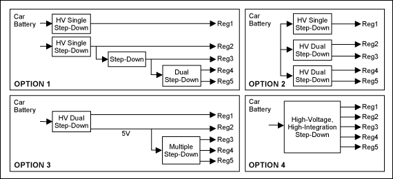
Figure 3. Architectural options for a power supply. Reg1: 8V (CD/DVD drive); Reg2: 5V (µC); Reg3: 3.3V (µC); Reg4: 2.5V/1.8V (DSP); Reg5: 1.2V (memory).
Just like its digital CMOS cousin, the analog BiCMOS processes also strive to minimize design geometry to achieve shrinkage. This relationship brings the best return on investment and lowers process development risks. Nonetheless, the process optimization choices do not necessarily match the needs of common automotive applications. For example, while 5.5V to 6V input devices are optimized for cost in most processes, the 9V to 10V input devices either do not exist or are not optimized for cost. This is why there are restrictions for how you can generate an intermediary power rail to cascade lower voltage rails.
The four topologies suggested in this section summarize our worldwide application design experience over the last three years. While there may be many more and different ways of achieving the objective, most solutions can be reduced to one of these four topologies.
Option 1
This topology maximizes the flexibility to optimize DC-DC conversion efficiency, location, heat distribution on the PCB, and noise. The principal advantages of Option1 are:
- Flexibility to add rails to a core design. The design provides optional rails for different projects. Even if it is not the lowest cost/highest efficiency solution, adding a single-output converter can help recycle a legacy design.
- The ability to optimize the choice of switcher/linear supplies. For example, if there is a 3.3V rail present in the system to power the microcontroller, it may make sense to use an LDO to generate a 1.8V 300mA rail from the 3.3V instead of from the car battery. If the rails change in time due to new requirements, one can easily select a new building block without significant cost penalty when the old block becomes less than optimal.
- Distributes the heat on the PCB, providing flexibility to select how much and where converters should dissipate heat.
- Enables use of high-performance and cost-efficient low-voltage analog ICs, which are also more widely available compared to high-voltage ICs.
Alternatively, one should note that Option 1 typically has a larger footprint, is more expensive, and is too complicated for designs with many power rails.
Option 2
This option is a popular compromise between higher integration and design flexibility. Typically the cost, footprint, and complexity with this approach are more optimal than Option 1.
This option is especially ideal for generating two step-down rails that need to be independently controlled. For example, an always-on 3.3V rail and a 5V rail that may be turned off can be generated using the same IC to save IQ. Another example is to generate an intermediary power rail, such as 5V, to supply lower voltage converters while avoiding boost circuitry to generate an 8V rail.
For dual-output regulators with external FET drivers, the heat distribution on the PCB is as flexible as Option 1. With internal FET converters, however, the concentration of heat dissipation at a particular point on the PCB can be restrictive depending on the current level required from the regulator output.
Option 3
This topology reduces the multiple-rail high-voltage conversion problem down to one high-voltage front-end and a highly integrated low-voltage, high-integration IC.
This approach simplifies the power-supply design and facilitates many alternative solutions from many different vendors. Also, low-voltage high-integration ICs are less expensive than multiple high-voltage ICs.
If the low-voltage PMIC of the Option 3 has more than two outputs, all the pitfalls of Option 4 are also present in Option 3.
The main disadvantage of Option3 is the many power rails concentrated at one place. This layout requires the design to manage heat dissipation on the PCB.
Option 4
All-in-one, high-integration PMICs can result in significantly better tradeoff among power-supply design constraints. There are, however, many pitfalls in high integration as well.
- Scalability and level of integration will always be at odds in a high-integration PMIC. For example, an internal FET converter may not be able to supply a heavier load as applications evolve from project to project.
- Cascading lower voltage converters to higher voltage ones can result in better cost. This approach can, however, restrict permutations of converter on/off logic. For example, a design that cascades a 3.3V input converter to a 5V output converter will have higher IQ, if the 3.3V rail has to be on when the 5V rail can be turned off.
- EMI and point-of-load conversion concerns can restrict use of a central PMIC. Board layout and use of long traces may inhibit which rails can be included in a central PMIC.
Maxim's Automotive Power Solutions
Maxim's automotive power-supply IC family provides unique high-performance solutions to hard-to-solve power-management problems. The power product family includes building blocks such as overvoltage and undervoltage protectors, microcontroller supervisors, switching and linear converters, and high-integration multifunction PMICs that meet the requirements of infotainment electronics design.
Maxim holds TS16949 (Automotive Quality Standard) certification and manufactures most of its parts in company-owned fabs. Maxim automotive operation has dedicated quality assurance, customer service, local sales and application support, and IC design resources to meet demands of the automotive market.
Maxim's power-supply ICs also address automotive specific quality or manufacturing needs such as AECQ100 qualification, DFMEA, different temperature grades (85°C, 105°C, 125°C, etc), special packaging (exposed leads or QFN, exposed pads or nonexposed pad).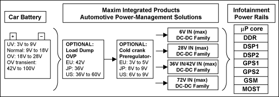
Figure 4. Automotive power-management IC categories. For full selection of Automotive power solutions please refer to www.maxim-ic.com/Automotive.
High-Voltage Single-Output PWM Controller
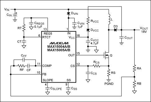
Figure 5. The MAX15004/MAX15005 automotive VFD power supplies operate down to a 2.5V input voltage after startup and includes output overvoltage protection for VFDs.
The MAX15004/MAX15005 are versatile current-mode PWM controllers that can be configured as boost, flyback, forward, and SEPIC converters. The ICs operate over the 4.5V to 40V input voltage range with an adjustable switching frequency from 15kHz to 500kHz. The ICs can also be synchronized to an external clock.
The current-mode control architecture offers excellent line-transient response and cycle-by-cycle current limit, while simplifying the frequency compensation. Programmable slope compensation simplifies the design further. A fast 60ns current-limit response time and low 300mV current-limit threshold make the controllers suitable for high-efficiency, high-frequency DC-DC converters. The devices include an internal error amplifier and 1% accurate reference to facilitate the primary-side regulated, single-ended flyback converter or nonisolated converters.
Protection features include cycle-by-cycle and hiccup current limit, output overvoltage protection, and thermal shutdown. The MAX15004/MAX15005 are available in a 16-pin TSSOP package with exposed pad and no exposed pad versions. All devices operate over the -40°C to +125°C automotive temperature range.
High-Voltage Single-Output, Step-Down Switching Controller
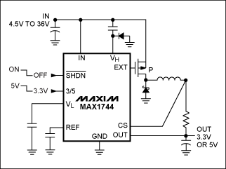
Figure 6. The MAX1744/MAX1745 are high-voltage (36V) step-down DC-DC controllers.
The MAX1744 is a single-output, automotive-grade switching regulator that withstands transients from 4.5V to 36V. The device uses a proprietary current-limited control scheme for excellent light and full load efficiency. It delivers more than 50W of output power without requiring a heatsink. The MAX1745 consumes only 4µA during shutdown and 90µA during a light load. The IC is fully specified for +125°C operation and is available in a 3mm x 3mm, 16-pin µMAX® package, which has exposed leads and no exposed pads. MAX1745 offers a resistor-adjustable output voltage.
High-voltage Single-Output LDO
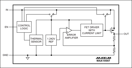
Figure 7. The MAX15006/MAX15007 are low 9µA quiescent-current linear regulators ideal for always-on automotive applications.
The MAX15006/MAX15007 are ultra-low quiescent-current linear regulators that operate from an input voltage of 4V to 40V. The ICs deliver up to 50mA of output current, and consume only 10µA of IQ at no load. The internal p-channel pass device keeps the IQ low even at full load. The MAX15007 consumes only 3µA current when in shutdown.
The MAX15006A/MAX15007A have a fixed 3.3V output, while the MAX15006B/MAX15007B have a fixed 5V output voltage. The MAX15007 includes an enable input to turn the device on or off. All devices are short-circuit protected and include thermal shutdown.
The MAX15006/MAX15007 operate over the -40°C to +125°C automotive temperature range. These devices are available in space-saving 3mm x 3mm, 6-pin TDFN and 8-pin SO thermally enhanced packages.
High-Voltage Dual-Output, Step-Down/Up Switching Converter
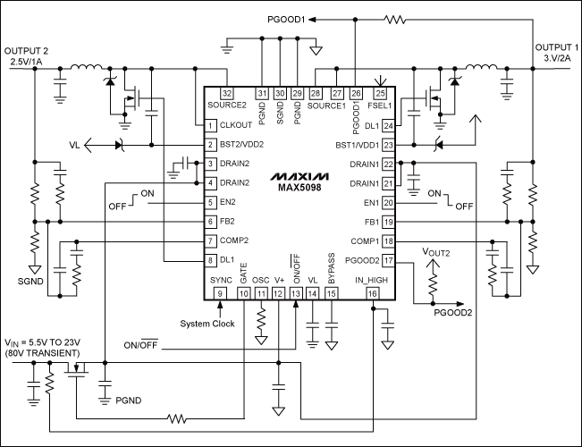
Figure 8. The MAX5098/MAX5099 withstand 80V load-dump and operate to less than 6V cold crank.
The MAX5098/MAX5099 are 2.2MHz, 180° out-of-phase dual-output switching regulators with internal high-side FETs. The ICs operate over a 4.5V to 19V input voltage range and integrate load-dump protection circuitry capable of handling load-dump transients up to 80V. The MAX5099 also integrates two low-side MOSFET drivers to allow each converter to drive an external synchronous rectifier MOSFET. Outputs 1 and 2 deliver up to 2A and 1A output current, respectively. The MAX5098 can be configured as a step-up or step-down converter; the MAX5099 operates only in step-down mode.
The MAX5098/MAX5099 also feature short-circuit (hiccup current limit) and thermal protection. The ICs operate over -40°C to +125°C and are available in a thermally enhanced, exposed pad, 5mm x 5mm, 32-pin TQFN or 28-pin TSSOP package.
A German version of this article appeared in the June 2008 edition of Automobil Elektronik.
¹ Please note that in ECORUN conditions the car engine is stopped temporarily (e.g., while waiting for the traffic light). This condition is also called start-stop or warm crank in the industry.
 電子發(fā)燒友App










評論