Compensating for the Nonlinear APD Response
Abstract:?Optical laser modules require compensation for the nonlinear response of the APD (avalanche photodiode). This application note discusses how Maxim's optical controllers are designed to compensate for this behavior. The DS1875 SFP controller serves as the example device in this article.
APD Characteristics
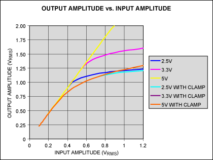
Optical modules use APD- (avalanche photodiode) based optical receivers for high-sensitivity applications.The feedback received from the APD diode is nonlinear (average received power). This nonlinearity makes it difficult to achieve good control of the laser module. Characteristics of typical APD nonlinearity are as shown in Figure 1.
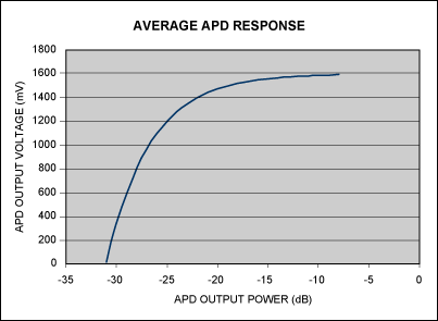
Figure 1. Typical APD performance shows a nonlinear response.
For proper operation it is necessary to compensate for this nonlinear behavior. This compensation allows for a linear feedback into the SFP controller module and increases the system's stability. The compensation response would then appear as shown in Figure 2.
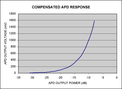
Figure 2. This is an average curve indicative of the expected typical response. Compensating for small variations in the response during production will not be feasible.
Using RSSI to Correct the Nonlinearity
Maxim's optical controllers like the DS1875 can compensate for the nonlinear behavior of APDs.One of the DS1875's input channels (MON3) has two ranges (fine and coarse), each with an independent scale and offset, to correct for the nonlinearity of the received power. This correction is done by a piecewise linear approximation of the nonlinear APD diode response.
In addition to providing two independent ranges, the DS1875 allows for right shifting of its ADC result for the fine range. By right shifting, increased resolution can be obtained, even though the input signal does not cover the entire input range.
Importance of Hysteresis
The DS1875 automatically switches between the two ranges depending on the magnitude of the input signal at a given crossover point. Hysteresis is provided at the crossover point, and it changes when going from the coarse range to the fine range. This ensures that the device does not toggle between the ranges and cause instability.Depending on the right shifting programmed for the fine range, the crossover point varies. Table 1 details how the crossover point changes for various settings of the right shifting. Note the changing values in the DEC column to the Hysteresis column.
Table 1. Settings for the Crossover Point with Right Shifting
| Right Shift | HEX | DEC | Hysteresis |
| 0 | FFF8 | 65528 | 61440 |
| 1 | 7FFC | 32764 | 30720 |
| 2 | 3FFE | 16382 | 15360 |
| 3 | 1FFF | 8191 | 7680 |
| 4 | FFF | 4095 | 3840 |
| 5 | 7FF | 2047 | 1920 |
| 6 | 3FF | 1023 | 960 |
| 7 | 1FF | 511 | 480 |
Calibrating the DS1875
The two ranges for the DS1875's MON3 input must be calibrated, so they correctly approximate the required APD response. Using the following process, the scale and offset values are identified for the two different ranges.- Make sure that the fine and the coarse ranges are programmed so that the effective response of each range is linear. The factory-programmed values are set so that the response is linear, with a right shift for the fine range of 3.
- Force two inputs ("a" dB and "b" dB) on MON3P. Using the factory calibration, measure the digital MON3 value. The two inputs are already configured so that the coarse range uses "a" dB and the fine range uses "b" dB. Any two points, one in the fine range and the other in the coarse range, can be chosen. Depending on the error identified, these measurements will have to be reevaluated to get the best piecewise linear approximation.
- The values obtained in step 2 will differ from the desired values to compensate the APD nonlinear response. The fine and coarse scale and offset values will all have to be calibrated so they properly match the desired values.
- The two measured values are considered "x" values. The desired outputs for the two points are considered "y" values.
- Calculate the scale and offset for the fine ADC range. Two points will be used for this calculation. The first point is the x value and y value (x1, y1) for the b dB input measured in the first calculation (step 2). The other is the (0, 0) point (x2, y2). The 0, 0 point is an assumption which allows us to trim the scales and offsets with just two data points. The user may want to use another data point if (0, 0) does not suit the desired response.
The calculation is done by:y = m_fine × x + c_fine
Where m_fine is the scale and c_fine is the offset
Using point (x2, y2), we get:c_fine = 0
Using point (x1, y1), we get:m_fine = y1/x1
- For the response desired, find the closest right shift required. Compare the desired output (the y value for point b dB) with the DEC values in Table 1. The DEC value closest to the desired response should be used as the x value. The corresponding desired (y) value should be calculated using the m_fine and c_fine values from above. This point is (x2, y2).
- Using the (x2, y2) cross values as a data point and the values for the b db point (x3, y3), calculate the scale and offset for the coarse ADC range by using:
y = m_coarse × x + c_coarse
- Load the offsets (c_fine and c_coarse) into the corresponding registers in the DS1875. Please note that if the offset values are negative, the 2's complement values are programmed into the registers.
- The fine and coarse scale values now have to be individually trimmed to read the desired values for the two inputs (a dB and b dB).
- An error curve can be generated (Figure 3) based on the modified response (using the new scale and offset values) and the desired response. The error curve can be changed depending on the position of the two points (a and b). The first lobe represents the error in the fine range; the second lobe represents the error in the coarse range. Changing the points will allow error magnitudes to be manipulated to suit the needs of the end user.
Results
The new fine and coarse values can be used to see if the device approximates the desired responses. Figure 3 shows the results for the response in Figure 2.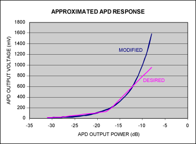
Figure 3. This error curve shows the modified response using the new scale and offset values and the desired response.
The error between the desired and the calculated response is shown in Figure 4.
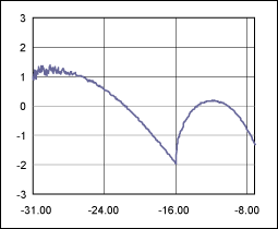
Figure 4. Error after the desired response was calculated.
 電子發(fā)燒友App








評(píng)論