Abstract: A combination of current-sense amplifier, dual-comparator and external CMOS switches can be used to prevent the damaging effects of a reversed-polarity battery or short-circuit load.
The most widely used device for overcurrent protection is a simple fuse. High current due to an overload heats the fusible metallic link, causing it to melt and open the circuit. The fuse is simple and economical. However, fuses' relatively long reaction time, high resistance, and need for replacement make them impractical for some applications.
A logic-controlled switch can provide low-loss switching and low quiescent current in addition to output short-circuit protection (Figure 1). The regulated charge pump (IC1) generates a gate drive of VBATT+10V for the NMOS FET switch, Q1. You turn on the circuit by applying VBATT to the on/off input. VOUT (pins 9 and 10) then pumps up to (VBATT+10V) within a millisecond or so, providing power to the op amp (IC2). To ensure that Q1 remains off until sufficient gate drive is available, a threshold detector in IC1 triggers a 0V-to-VBATT transition at the PR terminal (pin 6 of IC1) when the rising output equals VCC+8V.
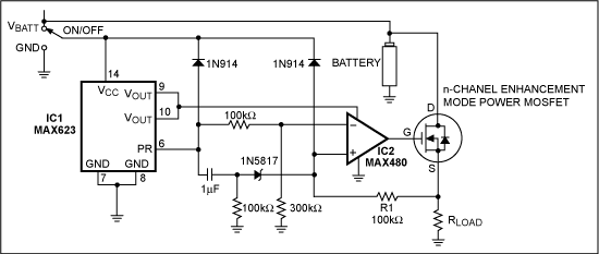
Figure 1. This logic-controlled switch circuit provides short-circuit protection at RLOAD.
The appearance of VBATT at the PR terminal produces 0.75×VBATT at the op amp's inverting input and a 100msec pulse at the noninverting input. The pulse kicks Q1 into conduction, and Q1 stays on as long as the source voltage remains more positive than the op amp's inverting input. Feedback through R1 provides short-circuit protection. If high load current pulls the source voltage below the reference level at the inverting input, the gate drive goes low and turns off Q1. The collapsing load voltage then latches off the switch. To reset, pull the on/off input to ground for at least 100msec and then back to VBATT.
In the circuit in Figure 2, one PMOS FET, Q1, provides passive protection against battery reversal, and a second MOSFET, Q3, disconnects the load from the battery in the event of excessive forward current flow. You should orient the MOSFETs' body diodes to prevent current flow when either device is off, regardless of the battery polarity.
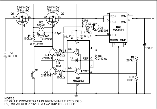
Figure 2. This circuit blocks the effect of a reversed-polarity battery or short-circuited load. R1 sets the current-limit threshold.
Q1, for example, connects backward (with respect to conventional practice) to align its body diode in the direction of normal current flow. A properly installed battery pulls Q1's gate more than 5V below its source, turning on Q1. A reversed battery drags the gate above the source, blocking current flow by reverse-biasing the body diode.
The current-sense amplifier, IC2, produces a small output current at pin 8 that is proportional to the current flowing between the RS+ and RS- terminals. The resulting voltage across R1 controls comparator B in IC1. During normal operation, Q3 remains on, because both comparator outputs are high. When the load current causes sufficient voltage across R1 to trip the B comparator, Q3 turns off and disconnects the battery from the load. At the same time, Q5 pulls the B comparator's inverting input to the supply rail, latching Q3 off as the supply rail falls. Q2 speeds the turn-off of Q3.
Comparator A acts as a safety valve that turns off Q3 in the event of a rapid short circuit. (In the absence of Q3, a short circuit causes oscillation: The initial increase in load current drives Q4 on and Q3 off, and the resulting loss of supply voltage kills IC2, allowing Q3 to turn on again.) R1 sets the current limit at 0A to 3A, according to the following equation, where 2000 is a gain factor internal to IC2, and VTH is the threshold of the comparators in IC1:
A similar version of this article appeared in the March 1, 1996 issue of EDN.
The most widely used device for overcurrent protection is a simple fuse. High current due to an overload heats the fusible metallic link, causing it to melt and open the circuit. The fuse is simple and economical. However, fuses' relatively long reaction time, high resistance, and need for replacement make them impractical for some applications.
A logic-controlled switch can provide low-loss switching and low quiescent current in addition to output short-circuit protection (Figure 1). The regulated charge pump (IC1) generates a gate drive of VBATT+10V for the NMOS FET switch, Q1. You turn on the circuit by applying VBATT to the on/off input. VOUT (pins 9 and 10) then pumps up to (VBATT+10V) within a millisecond or so, providing power to the op amp (IC2). To ensure that Q1 remains off until sufficient gate drive is available, a threshold detector in IC1 triggers a 0V-to-VBATT transition at the PR terminal (pin 6 of IC1) when the rising output equals VCC+8V.

Figure 1. This logic-controlled switch circuit provides short-circuit protection at RLOAD.
The appearance of VBATT at the PR terminal produces 0.75×VBATT at the op amp's inverting input and a 100msec pulse at the noninverting input. The pulse kicks Q1 into conduction, and Q1 stays on as long as the source voltage remains more positive than the op amp's inverting input. Feedback through R1 provides short-circuit protection. If high load current pulls the source voltage below the reference level at the inverting input, the gate drive goes low and turns off Q1. The collapsing load voltage then latches off the switch. To reset, pull the on/off input to ground for at least 100msec and then back to VBATT.
In the circuit in Figure 2, one PMOS FET, Q1, provides passive protection against battery reversal, and a second MOSFET, Q3, disconnects the load from the battery in the event of excessive forward current flow. You should orient the MOSFETs' body diodes to prevent current flow when either device is off, regardless of the battery polarity.

Figure 2. This circuit blocks the effect of a reversed-polarity battery or short-circuited load. R1 sets the current-limit threshold.
Q1, for example, connects backward (with respect to conventional practice) to align its body diode in the direction of normal current flow. A properly installed battery pulls Q1's gate more than 5V below its source, turning on Q1. A reversed battery drags the gate above the source, blocking current flow by reverse-biasing the body diode.
The current-sense amplifier, IC2, produces a small output current at pin 8 that is proportional to the current flowing between the RS+ and RS- terminals. The resulting voltage across R1 controls comparator B in IC1. During normal operation, Q3 remains on, because both comparator outputs are high. When the load current causes sufficient voltage across R1 to trip the B comparator, Q3 turns off and disconnects the battery from the load. At the same time, Q5 pulls the B comparator's inverting input to the supply rail, latching Q3 off as the supply rail falls. Q2 speeds the turn-off of Q3.
Comparator A acts as a safety valve that turns off Q3 in the event of a rapid short circuit. (In the absence of Q3, a short circuit causes oscillation: The initial increase in load current drives Q4 on and Q3 off, and the resulting loss of supply voltage kills IC2, allowing Q3 to turn on again.) R1 sets the current limit at 0A to 3A, according to the following equation, where 2000 is a gain factor internal to IC2, and VTH is the threshold of the comparators in IC1:
ILIMIT = 2000 × VTH/R1.
A similar version of this article appeared in the March 1, 1996 issue of EDN.
 電子發燒友App










評論