Abstract: A portable device using the circuit of Figure 1 derives power from the USB bus. The MAX1811 uses USB power charges a lithium-ion (Li+) battery at, USB compatible, 100mA or 500mA rates. Battery power is then stepped up with the MAX1747 to create the 5V supply rail. The 5V supply rail is then stepped down with the MAX1837 to create the 3.3V supply rail. The circuit includes a low battery shutdown to protect the Li+ battery and offers a convenient charging LED.
The Figure 1 circuit is powered by a universal serial bus (USB) port. It produces +5V and +3.3V to power portable devices such as digital cameras, MP3 players, and PDAs. It allows the port to maintain communications while supplying power, e.g., to charge a Li+ battery. IC2 boosts the battery voltage (VBATT) to 5V, and IC3 bucks that 5V output down to 3.3V.
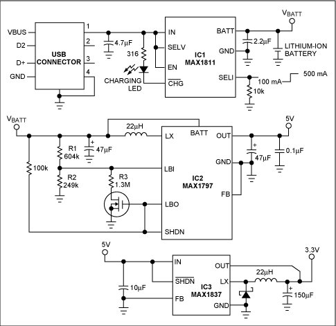
Figure 1. Drawing power from a USB port, this circuit generates +5V and +3.3V supply voltages for portable applications.
IC1 (a Li+ battery charger) draws power from the USB port to charge the battery. Pulling its SELI terminal low sets the charging current to 100mA for low-power USB ports, and pulling SELI high sets 500mA for high-power ports. Similarly, pulling SELV high or low configures the chip for charging a 4.2V or 4.1V Li+ battery. To protect the battery, IC1's final charging voltage exhibits 0.5% accuracy. The /CHG terminal allows the chip to illuminate an LED during charging.
IC2 is a step-up DC-DC converter that boosts VBATT to 5V and delivers up to 450mA. Its low-battery detection circuitry and true shutdown capability protects the Li+ battery. (By disconnecting the battery from the output, "true" shutdown limits battery current to less than 2μA.) The low-battery trip point is set by an external resistive divider between VBATT and GND, connected to LBI. Connecting the low-battery output (LBO) to shutdown (SHDN) causes IC2 to disconnect its load in response to a low battery voltage.
The internal source impedance of a Li+ battery makes IC2 susceptible to oscillation when its low-battery detection circuitry disconnects a low-voltage battery from its load: as the voltage drop across the battery's internal resistance is removed, the battery voltage increases and turns IC2 back on. For example, a Li+ battery with 500mΩ internal resistance, sourcing 500mA, drops 250mV across its internal resistance. When IC2 circuitry disconnects the load, forcing the battery current to zero, the battery voltage immediately increases by 250mV.
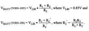
The n-channel FET at LBO eliminates this oscillation by adding hysteresis to the low-battery detection circuitry. The circuit shown is configured for a low-battery trip voltage of 2.9V. When VBATT goes below 2.9V, LBO opens and allows SHDN to be pulled high, turning on the FET. With the FET turned on, the parallel combination of 1.3MΩ and 249kΩ eliminates oscillation by setting the battery turn-on voltage to 3.3V.
A similar version of this article appeared in the December 20, 2001 issue of EDN magazine.
The Figure 1 circuit is powered by a universal serial bus (USB) port. It produces +5V and +3.3V to power portable devices such as digital cameras, MP3 players, and PDAs. It allows the port to maintain communications while supplying power, e.g., to charge a Li+ battery. IC2 boosts the battery voltage (VBATT) to 5V, and IC3 bucks that 5V output down to 3.3V.

Figure 1. Drawing power from a USB port, this circuit generates +5V and +3.3V supply voltages for portable applications.
IC1 (a Li+ battery charger) draws power from the USB port to charge the battery. Pulling its SELI terminal low sets the charging current to 100mA for low-power USB ports, and pulling SELI high sets 500mA for high-power ports. Similarly, pulling SELV high or low configures the chip for charging a 4.2V or 4.1V Li+ battery. To protect the battery, IC1's final charging voltage exhibits 0.5% accuracy. The /CHG terminal allows the chip to illuminate an LED during charging.
IC2 is a step-up DC-DC converter that boosts VBATT to 5V and delivers up to 450mA. Its low-battery detection circuitry and true shutdown capability protects the Li+ battery. (By disconnecting the battery from the output, "true" shutdown limits battery current to less than 2μA.) The low-battery trip point is set by an external resistive divider between VBATT and GND, connected to LBI. Connecting the low-battery output (LBO) to shutdown (SHDN) causes IC2 to disconnect its load in response to a low battery voltage.
The internal source impedance of a Li+ battery makes IC2 susceptible to oscillation when its low-battery detection circuitry disconnects a low-voltage battery from its load: as the voltage drop across the battery's internal resistance is removed, the battery voltage increases and turns IC2 back on. For example, a Li+ battery with 500mΩ internal resistance, sourcing 500mA, drops 250mV across its internal resistance. When IC2 circuitry disconnects the load, forcing the battery current to zero, the battery voltage immediately increases by 250mV.
The n-channel FET at LBO eliminates this oscillation by adding hysteresis to the low-battery detection circuitry. The circuit shown is configured for a low-battery trip voltage of 2.9V. When VBATT goes below 2.9V, LBO opens and allows SHDN to be pulled high, turning on the FET. With the FET turned on, the parallel combination of 1.3MΩ and 249kΩ eliminates oscillation by setting the battery turn-on voltage to 3.3V.
Finally, a step-down converter (IC3) bucks 5V to 3.3V, and delivers up to 250mA with efficiency exceeding 90%.
A similar version of this article appeared in the December 20, 2001 issue of EDN magazine.
 電子發燒友App







評論