優勢和特點
- 信噪比(SNR):71.8 dBc(72.8 dBFS�,至70 MHz��、125 MSPS)
- 無雜散動態范圍(SFDR):85 dBc (至70 MHz�、125 MSPS)
- 低功耗:750 mW (125 MSPS)
- 信噪比(SNR):71.6 dBc(72.6 dBFS�,至70 MHz、150 MSPS)
- 無雜散動態范圍(SFDR):84 dBc (至70 MHz��、150 MSPS)
- 低功耗:820 mW (150 MSPS)
- 1.8 V模擬電源供電
- 1.8 V至3.3V CMOS輸出電源或1.8 V LVDS輸出電源
- 1至8整數輸入時鐘除法器
- 中頻采樣頻率達450 MHz
- ADC內部基準電壓源
- 集成ADC采樣保持輸入
- 靈活的模擬輸入范圍:1 V p-p至2 V p-p
- 欲了解更多特性��,請參考數據手冊
產品詳情
The AD9640 is a dual 14-bit, 80/105/125/150 MSPS analog-to-digital converter (ADC). The AD9640 is designed to support communications applications where low cost, small size, and versatility are desired.
The dual ADC core features a multistage, differential pipelined architecture with integrated output error correction logic. Each ADC features wide bandwidth differential sample-and-hold analog input amplifiers supporting a variety of user-selectable input ranges. An integrated voltage reference eases design considerations. A duty cycle stabilizer is provided to compen-sate for variations in the ADC clock duty cycle, allowing the converters to maintain excellent performance.
The AD9640 has several functions that simplify the automatic gain control (AGC) function in the system receiver. The fast detect feature allows fast overrange detection by outputting four bits of input level information with very short latency.
In addition, the programmable threshold detector allows moni-toring of the incoming signal power using the four fast detect bits of the ADC with very low latency. If the input signal level exceeds the programmable threshold, the fine upper threshold indicator goes high. Because this threshold is set from the four MSBs, the user can quickly turn down the system gain to avoid an overrange condition.
The second AGC-related function is the signal monitor. This block allows the user to monitor the composite magnitude of the incoming signal, which aids in setting the gain to optimize the dynamic range of the overall system.
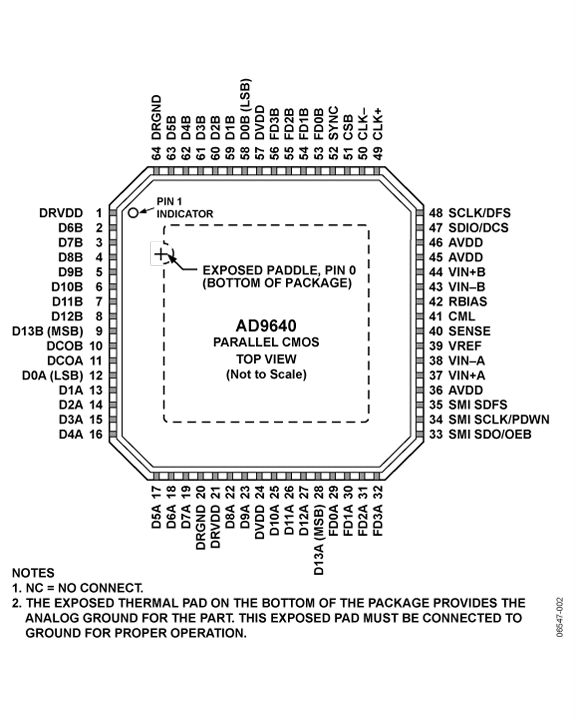
The ADC output data can be routed directly to the two external 14-bit output ports. These outputs can be set from 1.8 V to 3.3 V CMOS or 1.8 V LVDS.
Flexible power-down options allow significant power savings, when desired.
Programming for setup and control is accomplished using a 3-bit SPI-compatible serial interface.
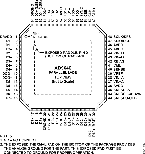
The AD9640 is available in a 64-lead LFCSP and is specified over the industrial temperature range of ?40°C to +85°C.
Product Highlights
- Integrated dual 14-bit, 80/105/125/150 MSPS ADC.
- Fast overrange detect and signal monitor with serial output.
- Signal monitor block with dedicated serial output mode.
- Proprietary differential input that maintains excellent SNR performance for input frequencies up to 450 MHz.
- Operation from a single 1.8 V supply and a separate digital output driver supply to accommodate 1.8 V to 3.3 V logic families.
- A standard serial port interface that supports various product features and functions, such as data formatting (offset binary, twos complement, or gray coding), enabling the clock DCS, power-down, and voltage reference mode.
- Pin compatibility with the AD9627, AD9627-11, and the AD9600 for a simple migration from 14 bits to 12 bits, 11 bits, or 10 bits.
Applications
- Communications
- Diversity radio systems
- Multimode digital receivers
GSM, EDGE, WCDMA, LTE,
CDMA2000, WiMAX, TD-SCDMA - I/Q demodulation systems
- Smart antenna systems
- General-purpose software radios
- Broadband data applications
方框圖


