| Architecture | Fixed Gain/Buffer |
| Number of channels (#) | 1 |
| Total supply voltage (Min) (+5V=5, +/-5V=10) | 5 |
| Total supply voltage (Max) (+5V=5, +/-5V=10) | 12 |
| GBW (Typ) (MHz) | 280 |
| BW @ Acl (MHz) | 280 |
| Acl, min spec gain (V/V) | 1 |
| Slew rate (Typ) (V/us) | 2100 |
| Vn at flatband (Typ) (nV/rtHz) | 1.7 |
| Vn at 1 kHz (Typ) (nV/rtHz) | 2 |
| Iq per channel (Typ) (mA) | 5.1 |
| Vos (offset voltage @ 25 C) (Max) (mV) | 2.5 |
| Rail-to-rail | No |
| Features | Shutdown |
| Rating | Catalog |
| Operating temperature range (C) | -40 to 85 |
| Input bias current (Max) (pA) | 45000000 |
| Offset drift (Typ) (uV/C) | 12 |
| Output current (Typ) (mA) | 190 |
| 2nd harmonic (dBc) | 79 |
| 3rd harmonic (dBc) | 94 |
| Frequency of harmonic distortion measurement (MHz) | 5 |
- FLEXIBLE SUPPLY RANGE:
- +5V to +12V Single Supply
- ±2.5V to ±6V Dual Supplies
- INTERNALLY FIXED GAIN: +2 or ±1
- HIGH BANDWIDTH (G = +2): 225MHz
- LOW SUPPLY CURRENT: 5.1mA
- LOW DISABLED CURRENT: 150 μA
- HIGH OUTPUT CURRENT: 190mA
- OUTPUT VOLTAGE SWING: ±4.0V
- SOT23-6 AVAILABLE
- APPLICATIONS
- BROADBAND VIDEO LINE DRIVERS
- MULTIPLE LINE VIDEO DA
- PORTABLE INSTRUMENTS
- ADC BUFFERS
- ACTIVE FILTERS
All trademarks are the property of their respective owners.
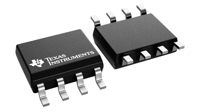
The OPA692 provides an easy to use, broadband fixed gain video buffer amplifier. Depending on the external connections, the internal resistor network may be used to provide either a fixed gain of +2 video buffer or a gain of +1 or ?1 voltage buffer. Operating on a very low 5.1mA supply current, the OPA692 offers a slew rate and output power normally associated with a much higher supply current. A new output stage architecture delivers high output current with a minimal headroom and crossover distortion. This gives exceptional single-supply operation. Using a single +5V supply, the OPA692 can deliver a 1V to 4V output swing with over 120mA drive current and > 200MHz bandwidth. This combination of features makes the OPA692 an ideal RGB line driver or single-supply Analog-to-Digital Converter (ADC) input driver.
The low 5.1mA supply current for the OPA692 is precisely trimmed at +25°C. This trim, along with low drift over temperature, ensures lower maximum supply current than competing products that report only a room temperature nominal supply current. System power may be further reduced by using the optional disable control pin. Leaving this disable pin open, or holding it HIGH, gives normal operation. If pulled LOW, the OPA692 supply current drops to less than 150 μA while the I/O pins go into a high impedance state.


