| Vin (Min) (V) | 1.8 |
| Vin (Max) (V) | 5.5 |
| Vout (Min) (V) | 3.3 |
| Vout (Max) (V) | 3.3 |
| Switch current limit (Typ) (A) | 1.3 |
| Regulated outputs (#) | 2 |
| Switching frequency (Min) (kHz) | 400 |
| Switching frequency (Max) (kHz) | 600 |
| Iq (Typ) (mA) | 0.04 |
| Features | Enable, Light Load Efficiency, Load Disconnect, Power Good |
| Duty cycle (Max) (%) | 100 |
| Rating | Catalog |
- Synchronous, Up to 90% Efficient, SEPIC
Converter With 300-mA Output Current From
2.5-V Input - Integrated 200-mA Reverse Voltage Protected
LDO for DC-DC Output Voltage Post Regulation
or Second Output Voltage - 40-μA (Typical) Quiescent Current
- Input Voltage Range: 1.8 V to 5.5 V
- Fixed and Adjustable Output Voltage Options up
to 5.5 V - Power Save Mode for Improved Efficiency at Low-
Output Power - Low Battery Comparator
- Power Good Output
- Low EMI-Converter (Integrated Antiringing Switch)
- Load Disconnect During Shutdown
- Overtemperature Protection
- Available in a Small 4-mm × 4-mm VQFN-16 or in
a TSSOP-16 Package - APPLICATIONS
- All Single Cell Li, Dual or Triple Cell Battery or
USB Powered Products as MP-3 Player, PDAs,
and Other Portable Equipment - Dual Input or Dual Output Mode
- High Efficient Li-Ion to 3.3-V Conversion
- All Single Cell Li, Dual or Triple Cell Battery or
All other trademarks are the property of their respective owners
The TPS6113x devices provide a complete power supply solution for products powered by either a one-cell Li-Ion or Li-Polymer, or two- to four-cell Alkaline, NiCd, or NiMH batteries. The devices can generate two regulated output voltages. It provides a simple and efficient buck-boost solution for generating 3.3 V out of an input voltage that can be both higher and lower than the output voltage. The converter provides a maximum output current of at least 300 mA with supply voltages down to 1.8 V. The implemented SEPIC converter is based on a fixed frequency, pulse-width-modulation (PWM) controller using a synchronous rectifier to obtain maximum efficiency. The maximum peak current in the SEPIC switch is limited to a value of 1600 mA.
The converter can be disabled to minimize battery drain. During shutdown, the load is completely disconnected from the battery. A low-EMI mode is implemented to reduce ringing, and in effect, lower radiated electromagnetic energy when the converter enters the discontinuous conduction mode. A power good output at the SEPIC stage provides additional control of any connected circuits like cascaded power supply stages, or microprocessors.
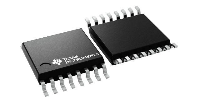
The built-in LDO can be used for a second output voltage derived either from the SEPIC output or directly from the battery. The output voltage of this LDO can be programmed by an external resistor divider or is fixed internally on the chip. The LDO can be enabled separately, that is, using the power good of the SEPIC stage. The device is packaged in a 16-pin VQFN package measuring 4 mm × 4 mm (RSA) or in a 16-pin TSSOP (PW) package.


