| Output options | Adjustable Output, Tracking Output |
| Iout (Max) (A) | 1.5 |
| Vin (Max) (V) | 5.5 |
| Vin (Min) (V) | 0.8 |
| Vout (Max) (V) | 3.6 |
| Vout (Min) (V) | 0.8 |
| Noise (uVrms) | 20 |
| Iq (Typ) (mA) | 3 |
| Thermal resistance θJA (°C/W) | 20 |
| Rating | Catalog |
| Load capacitance (Min) (μF) | 0 |
| Regulated outputs (#) | 1 |
| Features | Enable, Power good |
| Accuracy (%) | 1 |
| PSRR @ 100 KHz (dB) | 45 |
| Dropout voltage (Vdo) (Typ) (mV) | 55 |
| Operating temperature range (C) | -40 to 85 |
- Track Pin Allows for Flexible Power-Up Sequencing
- 1% Accuracy Over Line, Load, and Temperature
- Supports Input Voltages as Low as 0.9V with External Bias Supply
- Adjustable Output (0.8V to 3.6V)
- Fixed Output (0.9V to 3.6V)
- Ultra-Low Dropout: 55mV at 1.5A (typ)
- Stable with Any or No Output Capacitor
- Excellent Transient Response
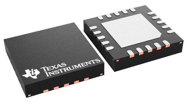
- Available in 5mm × 5mm × 1mm QFN and DDPAK-7 Packages
- Open-Drain Power-Good (5 × 5 QFN)
- Active High Enable
- APPLICATIONS
- FPGA Applications
- DSP Core and I/O Voltages
- Post-Regulation Applications
- Applications with Special Start-Up Time or Sequencing Requirements
All other trademarks are the property of their respective owners
The TPS743xx low-dropout (LDO) linear regulators provide an easy-to-use robust power management solution for a wide variety of applications. The TRACK pin allows the output to track an external supply. This feature is useful in minimizing the stress on ESD structures that are present between the CORE and I/O power pins of many processors. The enable input and power-good output allow easy sequencing with external regulators. This complete flexibility allows the user to configure a solution that meets the sequencing requirements of FPGAs, DSPs, and other applications with special start-up requirements.
A precision reference and error amplifier deliver 1% accuracy over load, line, temperature, and process. Each LDO is stable with low-cost ceramic output capacitors and the family is fully specified from –40°C to +125°C. The TPS743xx is offered in a small (5mm × 5mm) QFN package, yielding a highly compact total solution size. For applications that require additional power dissipation, the DDPAK (KTW) package is also available.


