關鍵詞: Cortex-M1 , IGLOO , Microsemi
Microsemi公司的Actel IGLOO低功耗全特性閃存FPGA能滿足當今手提設備所需求的功耗,面積和成本的嚴格需求. IGLOO系于支持多達300萬系數門,雙端口SRAM高達504kb,多達6個嵌入PLL和620個用戶I/O,工作電壓1.2V-1.5V,功耗低至5uW,主要用在智能手機,GPS,PDA,DCAM,手提工業和醫療設備,平板電腦,PCMCIA和任何超低功耗設備.本文介紹了IGLOO系列主要特性,以及Cortex-M1使能IGLOO開發套件主要特性,方框圖,電路圖,材料清單和PCB元件布局圖.
2012-3-13 13:04:25 上傳
The Actel IGLOO low-power FPGA family of reprogrammable, full-featured flash FPGAs is designed to meet the demanding power, area, and cost requirements of today’s portable electronics. Based on the Actel nonvolatile flash technology and single-chip ProASIC3 FPGA architecture, the 1.2 V to 1.5 V operating voltage family offers the industry’s lowest power consumption—as low as 5 µW. The IGLOO family supports up to 3 million system gates with up to 504 kbits of true dual-port SRAM, up to 6 embedded PLLs, and up to 620 user I/Os.
Low-power applications that require 32-bit processing can use the ARM® Cortex™-M1 processor without license fee or royalties in M1 IGLOO devices. Developed specifically for implementation in FPGAs, Cortex-M1 offers an optimal balance between performance and size to minimize power consumption.
The IGLOO family of flash FPGAs, based on a 130-nm flash process, offers the lowest power FPGA, a single-chip solution, small footprint packages, reprogrammability, and an abundance of advanced
M1AGL1000V2 主要特性:
The Flash*Freeze technology used in IGLOO devices enables entering and exiting an ultra-low power mode that consumes as little as 5 μW while retaining SRAM and register data. Flash*Freeze technology simplifies power management through I/O and clock management with rapid recovery to operation mode.
The Low Power Active capability (static idle) allows for ultra-low power consumption (from 12 μW) while the IGLOO device is completely functional in the system. This allows the IGLOO device to control system power management based on external inputs (e.g., scanning for keyboard stimulus) while consuming minimal power.
Nonvolatile flash technology gives IGLOO devices the advantage of being a secure, low power, singlechip solution that is live at power-up (LAPU). IGLOO is reprogrammable and offers time-to-market benefits at an ASIC-level unit cost.
These features enable designers to create high-density systems using existing ASIC or FPGA design flows and tools.
IGLOO devices offer 1 kbit of on-chip, reprogrammable, nonvolatile FlashROM storage as well as clock conditioning circuitry based on an integrated phase-locked loop (PLL). The AGL015 and AGL030 devices have no PLL or RAM support. IGLOO devices have up to 1 million system gates, supported with up to 144 kbits of true dual-port SRAM and up to 300 user I/Os.
M1 IGLOO devices support the high-performance, 32-bit Cortex-M1 processor developed by ARM for implementation in FPGAs. Cortex-M1 is a soft processor that is fully implemented in the FPGA fabric. It has a three-stage pipeline that offers a good balance between low power consumption and speed when implemented in an M1 IGLOO device. The processor runs the ARMv6-M instruction set, has a configurable nested interrupt controller, and can be implemented with or without the debug block. Cortex- M1 is available for free from Microsemi for use in M1 IGLOO FPGAs.
The ARM-enabled devices have ordering numbers that begin with M1AGL and do not support AES decryption.
Flash*Freeze Technology
The IGLOO device offers unique Flash*Freeze technology, allowing the device to enter and exit ultra-low power Flash*Freeze mode. IGLOO devices do not need additional components to turn off I/Os or clocks while retaining the design information, SRAM content, and registers. Flash*Freeze technology is combined with in-system programmability, which enables users to quickly and easily upgrade and update their designs in the final stages of manufacturing or in the field. The ability of IGLOO V2 devices to support a wide range of core voltage (1.2 V to 1.5 V) allows further reduction in power consumption, thus achieving the lowest total system power.
When the IGLOO device enters Flash*Freeze mode, the device automatically shuts off the clocks and inputs to the FPGA core; when the device exits Flash*Freeze mode, all activity resumes and data is retained.
The availability of low power modes, combined with reprogrammability, a single-chip and single-voltage solution, and availability of small-footprint, high pin-count packages, make IGLOO devices the best fit for portable electronics.
Features and Benefits
Low Power
• 1.2 V to 1.5 V Core Voltage Support for Low Power
• Supports Single-Voltage System Operation
• 5 μW Power Consumption in Flash*Freeze Mode
•Low Power Active FPGA Operation
•Flash*Freeze Technology Enables Ultra-Low Power Consumption while Maintaining FPGA Content
•Easy Entry to / Exit from Ultra-Low Power Flash*Freeze Mode High Capacity
• 15K to 1 Million System Gates
• Up to 144 Kbits of True Dual-Port SRAM
• Up to 300 User I/Os
Reprogrammable Flash Technology
• 130-nm, 7-Layer Metal, Flash-Based CMOS Process
• Live-at-Power-Up (LAPU) Level 0 Support
• Single-Chip Solution
• Retains Programmed Design When Powered Off
• 250 MHz (1.5 V systems) and 160 MHz (1.2 V systems) System Performance In-System Programming (ISP) and Security
• ISP Using On-Chip 128-Bit Advanced Encryption Standard
(AES) Decryption (except ARM®-enabled IGLOO® devices) via JTAG (IEEE 1532–compliant)†
• FlashLock® Designed to Secure FPGA Contents High-Performance Routing Hierarchy
• Segmented, Hierarchical Routing and Clock Structure Advanced I/O
• 700 Mbps DDR, LVDS-Capable I/Os (AGL250 and above)
• 1.2 V, 1.5 V, 1.8 V, 2.5 V, and 3.3 V Mixed-Voltage Operation
• Bank-Selectable I/O Voltages—up to 4 Banks per Chip
• Single-Ended I/O Standards: LVTTL, LVCMOS
3.3 V / 2.5 V / 1.8 V / 1.5 V / 1.2 V, 3.3 V PCI / 3.3 V PCI-X†, and LVCMOS 2.5 V / 5.0 V Input†
• Differential I/O Standards: LVPECL, LVDS, B-LVDS, and MLVDS (AGL250 and above)
• Wide Range Power Supply Voltage Support per JESD8-B,Allowing I/Os to Operate from 2.7 V to 3.6 V
• Wide Range Power Supply Voltage Support per JESD8-12, Allowing I/Os to Operate from 1.14 V to 1.575 V
• I/O Registers on Input, Output, and Enable Paths
• Hot-Swappable and Cold-Sparing I/Os‡
• Programmable Output Slew Rate† and Drive Strength
• Weak Pull-Up/-Down
• IEEE 1149.1 (JTAG) Boundary Scan Test
• Pin-Compatible Packages across the IGLOO Family Clock Conditioning Circuit (CCC) and PLL†
• Six CCC Blocks, One with an Integrated PLL
• Configurable Phase Shift, Multiply/Divide, Delay Capabilities, and External Feedback
• Wide Input Frequency Range (1.5 MHz up to 250 MHz) Embedded Memory
• 1 kbit of FlashROM User Nonvolatile Memory
• SRAMs and FIFOs with Variable-Aspect-Ratio 4,608-Bit† RAM Blocks (×1, ×2, ×4, ×9, and ×18 organizations)
• True Dual-Port SRAM (except ×18)†
ARM Processor Support in IGLOO FPGAs
• M1 IGLOO Devices—Cortex™-M1 Soft Processor Available with or without Debug Cortex-M1使能IGLOO開發套件
Cortex-M1–Enabled IGLOO Development Kit
The Cortex-M1–Enabled IGLOO Development Kit is an advanced microprocessor-based FPGA development and evaluation kit. The purpose of the kit is to help the user become familiar with the IGLOO FPGA features by providing a useful Sample Design, with a "How To" tutorial for implementing the FPGA hardware design using Microsemi Libero® Integrated Design Environment Project Manager.
The tutorial also shows how to implement Cortex-M1 embedded software using SoftConsole.
Cortex-M1使能IGLOO開發套件主要特性:
• Ultra-low power in Flash*Freeze mode
• Low-power active capability
• Small footprint packages
• Reprogrammable flash technology
• 1.2 V or 1.5 V operation
• High capacity, advanced I/O
• Clock conditioning circuit (CCC) and PLL
• Embedded SRAM and nonvolatile memory (NVM)
• In-system programming (ISP) and security
• Cortex-M1 processor
圖1.Cortex-M1使能IGLOO開發板外形圖
Cortex-M1使能IGLOO開發套件包括:
The Cortex-M1–Enabled IGLOO Development Kit includes the following:
• M1AGL Development Board
• Libero IDE v8.x DVD (in DVD case)
• Cortex-M1–Enabled IGLOO Development Kit Install CD with sample design
• +5.0 V external power supply with international adapters
• 2 USB A to Mini-B cables
• 4 self-adhesive rubber pads
• Quickstart Guide
Cortex-M1使能IGLOO開發套件主要應用:
• Smartphones, GPS, DCAM, PDA
• Portable industrial & medical equipment
• PC laptops, PCMCIA
• Any ultra-low power devices
2012-3-13 13:04:25 上傳
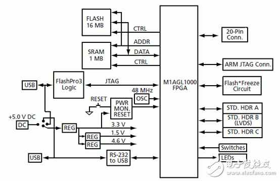
下載附件 (25.68 KB)圖2.Cortex-M1使能IGLOO開發板方框圖
2012-3-13 13:04:25 上傳
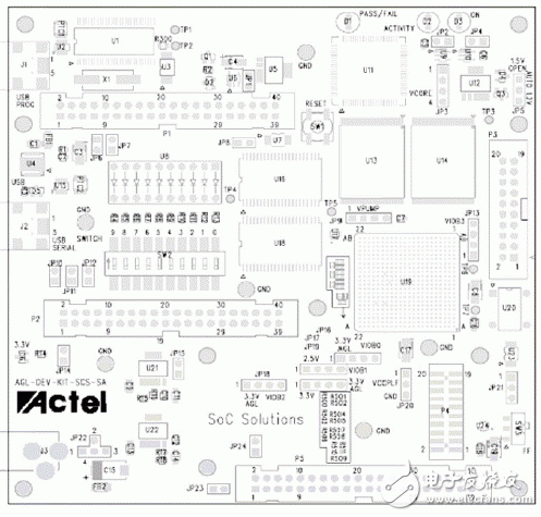
下載附件 (64.52 KB)圖3.Cortex-M1使能IGLOO開發板裝配圖(頂層)
ARM Cortex-M1 IGLOO Development Board with an M1AGL1000V2-FGG484 device
1 million system gates, M1AGL1000V2 device in FGG484 package
Oscillator for system clock is provided
Eight LEDs and eight switchesprovide simple inputs and outputs to the system
USB programming and debug connection
Second USB connection for USB-to-serial (RS232) interface, also allows powering of the board
Optional board power connector for an external supply, but none is needed when connected to a USB cable
Memory devices
4 MB of SRAM provided on board
16 MB of flash memory provided on board
General purpose I/O banks
Three 40-pin GPIO banks are provided for interfacing to other equipment. Two of these banks are fully populated.
Programmer built into board via USB 2.0 connection
2012-3-13 13:04:25 上傳
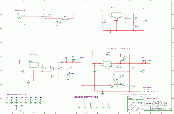
下載附件 (20.17 KB)圖4.Cortex-M1使能IGLOO開發板電路圖(1)
2012-3-13 13:04:25 上傳
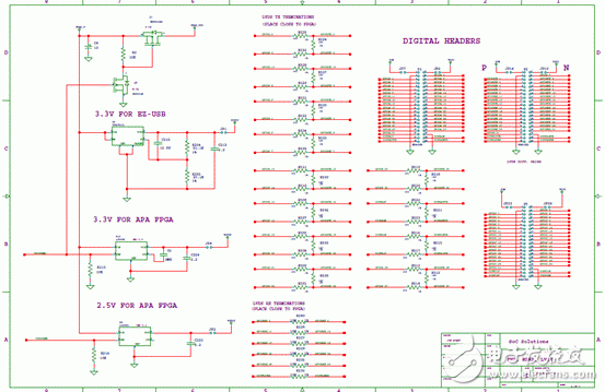
下載附件 (36.73 KB)圖5.Cortex-M1使能IGLOO開發板電路圖(2)
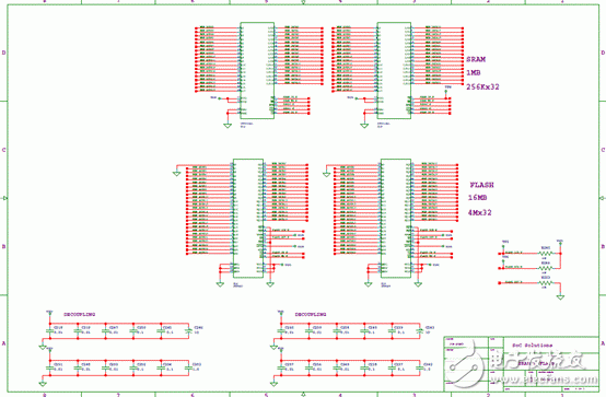
2012-3-13 13:04:25 上傳
下載附件 (33.94 KB)圖6.Cortex-M1使能IGLOO開發板電路圖(3)
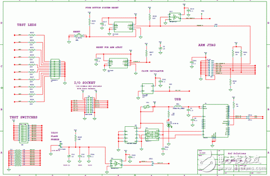
2012-3-13 13:04:25 上傳
下載附件 (34.51 KB)圖7.Cortex-M1使能IGLOO開發板電路圖(4)
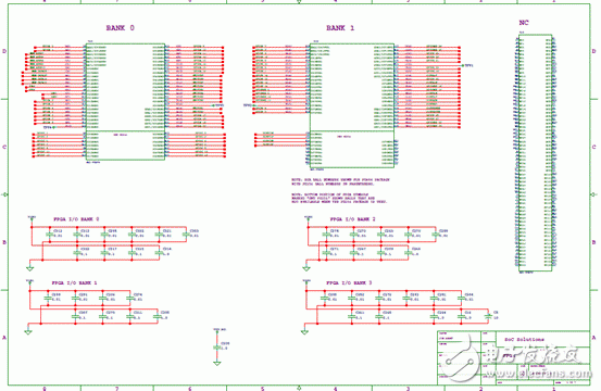
2012-3-13 13:04:25 上傳
下載附件 (36.31 KB)圖8.Cortex-M1使能IGLOO開發板電路圖(5)
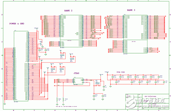
2012-3-13 13:04:25 上傳
下載附件 (44.81 KB)圖9.Cortex-M1使能IGLOO開發板電路圖(6)

2012-3-13 13:04:25 上傳
下載附件 (37.51 KB)圖10.Cortex-M1使能IGLOO開發板電路圖(7)
Cortex-M1使能IGLOO開發板材料清單見:
2012-3-13 13:15:49 上傳
下載附件 (138 Bytes) Cortex-M1使能IGLOO開發板材料清單.rar (12.15 KB, 下載次數: 0)
2012-3-13 13:14:42 上傳
下載次數: 0下載積分: 積分 -1
詳情請見:
IGLOO_DS[1].pdf (11.23 MB, 下載次數: 0)
2012-3-13 13:13:01 上傳
下載次數: 0下載積分: 積分 -1 和
M1IGLOO_DevKit_UG[1].pdf (3.55 MB, 下載次數: 0)
2012-3-13 13:14:22 上傳
下載次數: 0下載積分: 積分 -1
 電子發燒友App








評論