資料介紹
AD9644是一款14位雙通道模數轉換器(ADC),配有一個高速串行輸出接口,采樣速度可為80MSPS或155MSPS。這款雙通道ADC內核采用多級、差分流水線架構,并集成了輸出糾錯邏輯。每個ADC均具有寬帶寬、差分采樣保持模擬輸入放大器,支持用戶可選的各種輸入范圍。集成基準電壓源可簡化設計。占空比穩定器可用來補償ADC時鐘占空比的波動,使轉換器保持出色的性能。
控制理論
The AD9644 dual-core analog-to-digital converter (ADC) can be used for diversity reception of signals, in which the ADCs are operating identically on the same carrier but from two separate antennae. The ADCs can also be operated with independent analog inputs. The user can sample any fS/2 frequency segment from dc to 250 MHz, using appropriate low-pass or band-pass filtering at the ADC inputs with little loss in ADC performance.
In nondiversity applications, the AD9644 can be used as a base-band or direct downconversion receiver, in which one ADC is used for I input data, and the other is used for Q input data.
Synchronization capability is provided to allow synchronized timing between multiple devices. Programming and control of the AD9644 are accomplished using a 3-wire SPI-compatible serial interface.
模數轉換器結構
The AD9644 architecture consists of a dual front-end sample-and-hold circuit, followed by a pipelined, switched-capacitor ADC. The quantized outputs from each stage are combined into a final 14-bit result in the digital correction logic. The pipelined architecture permits the first stage to operate on a new input sample and the remaining stages to operate on the preceding samples. Sampling occurs on the rising edge of the clock.
Each stage of the pipeline, excluding the last, consists of a low resolution flash ADC connected to a switched-capacitor digital-to-analog converter (DAC) and an interstage residue amplifier (MDAC)。 The MDAC magnifies the difference between the recon-structed DAC output and the flash input for the next stage in the pipeline. One bit of redundancy is used in each stage to facilitate digital correction of flash errors. The last stage simply consists of a flash ADC.
The input stage of each channel contains a differential sampling circuit that can be ac- or dc-coupled in differential or single-ended modes. The output staging block aligns the data, corrects errors, and passes the data to the output buffers. The output buffers are powered from a separate supply, allowing digital output noise to be separated from the analog core. During power-down, the output buffers go into a high impedance state.
模擬輸入注意事項
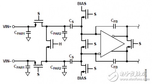
The analog input to the AD9644 is a differential switched-capacitor circuit that has been designed for optimum performance while processing a differential input signal.
The clock signal alternatively switches the input between sample mode and hold mode (see Figure 1)。 When the input is switched into sample mode, the signal source must be capable of charging the sample capacitors and settling within ? of a clock cycle.

Figure 1
A small resistor in series with each input can help reduce the peak transient current required from the output stage of the driving source. A shunt capacitor can be placed across the inputs to provide dynamic charging currents. This passive network creates a low-pass filter at the ADC input; therefore, the precise values are dependent on the application.
In intermediate frequency (IF) undersampling applications, any shunt capacitors or series resistors should be reduced since the input sample capacitor is unbuffered. In combination with the driving source impedance, the shunt capacitors limit the input bandwidth. Refer to the AN-742 Application Note, Frequency Domain Response of Switched-Capacitor ADCs; the AN-827 Application Note, A Resonant Approach to Interfacing Amplifiers to Switched-Capacitor ADCs; and the Analog Dialogarticle, “Transformer-Coupled Front-End for Wideband A/D Converters,” for more information on this subject (refer to www.analog.com)。
For best dynamic performance, the source impedances driving VIN+ and VIN? should be matched, and the inputs should be differentially balanced.
輸入模式
The analog inputs of the AD9644 are not internally dc biased. In ac-coupled applications, the user must provide this bias externally. Setting the device so that VCM = 0.5 × AVDD (or 0.9 V) is recommended for optimum performance. An on-board common-mode voltage reference is included in the design and is available from the VCMA and VCMB pins. Using the VCMA and VCMB outputs to set the input common mode is recommended. Optimum performance is achieved when the common-mode voltage of the analog input is set by the VCMA and VCMB pin voltages (typically 0.5 × AVDD)。 The VCMA and VCMB pins must be decoupled to ground by a 0.1 μF capacitor. This decoupling capacitor should be placed close to the pin to minimize the series resistance and inductance between the part and this capacitor.
控制理論
The AD9644 dual-core analog-to-digital converter (ADC) can be used for diversity reception of signals, in which the ADCs are operating identically on the same carrier but from two separate antennae. The ADCs can also be operated with independent analog inputs. The user can sample any fS/2 frequency segment from dc to 250 MHz, using appropriate low-pass or band-pass filtering at the ADC inputs with little loss in ADC performance.
In nondiversity applications, the AD9644 can be used as a base-band or direct downconversion receiver, in which one ADC is used for I input data, and the other is used for Q input data.
Synchronization capability is provided to allow synchronized timing between multiple devices. Programming and control of the AD9644 are accomplished using a 3-wire SPI-compatible serial interface.
模數轉換器結構
The AD9644 architecture consists of a dual front-end sample-and-hold circuit, followed by a pipelined, switched-capacitor ADC. The quantized outputs from each stage are combined into a final 14-bit result in the digital correction logic. The pipelined architecture permits the first stage to operate on a new input sample and the remaining stages to operate on the preceding samples. Sampling occurs on the rising edge of the clock.
Each stage of the pipeline, excluding the last, consists of a low resolution flash ADC connected to a switched-capacitor digital-to-analog converter (DAC) and an interstage residue amplifier (MDAC)。 The MDAC magnifies the difference between the recon-structed DAC output and the flash input for the next stage in the pipeline. One bit of redundancy is used in each stage to facilitate digital correction of flash errors. The last stage simply consists of a flash ADC.
The input stage of each channel contains a differential sampling circuit that can be ac- or dc-coupled in differential or single-ended modes. The output staging block aligns the data, corrects errors, and passes the data to the output buffers. The output buffers are powered from a separate supply, allowing digital output noise to be separated from the analog core. During power-down, the output buffers go into a high impedance state.
模擬輸入注意事項
The analog input to the AD9644 is a differential switched-capacitor circuit that has been designed for optimum performance while processing a differential input signal.
The clock signal alternatively switches the input between sample mode and hold mode (see Figure 1)。 When the input is switched into sample mode, the signal source must be capable of charging the sample capacitors and settling within ? of a clock cycle.

Figure 1
A small resistor in series with each input can help reduce the peak transient current required from the output stage of the driving source. A shunt capacitor can be placed across the inputs to provide dynamic charging currents. This passive network creates a low-pass filter at the ADC input; therefore, the precise values are dependent on the application.
In intermediate frequency (IF) undersampling applications, any shunt capacitors or series resistors should be reduced since the input sample capacitor is unbuffered. In combination with the driving source impedance, the shunt capacitors limit the input bandwidth. Refer to the AN-742 Application Note, Frequency Domain Response of Switched-Capacitor ADCs; the AN-827 Application Note, A Resonant Approach to Interfacing Amplifiers to Switched-Capacitor ADCs; and the Analog Dialogarticle, “Transformer-Coupled Front-End for Wideband A/D Converters,” for more information on this subject (refer to www.analog.com)。
For best dynamic performance, the source impedances driving VIN+ and VIN? should be matched, and the inputs should be differentially balanced.
輸入模式
The analog inputs of the AD9644 are not internally dc biased. In ac-coupled applications, the user must provide this bias externally. Setting the device so that VCM = 0.5 × AVDD (or 0.9 V) is recommended for optimum performance. An on-board common-mode voltage reference is included in the design and is available from the VCMA and VCMB pins. Using the VCMA and VCMB outputs to set the input common mode is recommended. Optimum performance is achieved when the common-mode voltage of the analog input is set by the VCMA and VCMB pin voltages (typically 0.5 × AVDD)。 The VCMA and VCMB pins must be decoupled to ground by a 0.1 μF capacitor. This decoupling capacitor should be placed close to the pin to minimize the series resistance and inductance between the part and this capacitor.
下載該資料的人也在下載
下載該資料的人還在閱讀
更多 >
- DAC8801:14位串行輸入乘法數模轉換器數據表
- AD9253:四路14位80 MSPS/105 MSPS/125 MSPS串行LVDS 1.8 V模數轉換器產品手冊
- AD9684:14位、500 MSPS LVDS、雙模數轉換器
- AD9681:八進制、14位、125 MSPS、串行LVDS、1.8 V模數轉換器數據表
- ADW12001:14位、40 MSPS雙模數轉換器數據表
- AD9644:14位、80 MSPS/155 MSPS、1.8 V雙串行輸出模數轉換器(ADC)產品手冊
- AD6645:14位、80 MSPS/105 MSPS模數轉換器
- AD9257:8通道、14位、40/65 MSPS串行LVDS 1.8 V模數轉換器
- AD9645: 雙通道、14位、80 MSPS/125 MSPS串行LVDS 1.8 V模數轉換器
- 具有采樣保持功能的低電壓8位串行接口CMOS模數轉換器ADCV0832的介紹 1次下載
- AD9644:14位串行模數轉換器入門必讀資料 1次下載
- 多通道14位串行AD轉換器MAX1148 13次下載
- 16位串行模數轉換器ADS8509及應用 155次下載
- 14位125Msps模數轉換器ADS5500及其應用
- 10位串行模數轉換芯片AD7810的原理及應用
- RA6T2的16位模數轉換器操作 [14] 驗證應用項目 248次閱讀
- RA6T2的16位模數轉換器操作 [13] 運行應用項目 224次閱讀
- 模數轉換器的技術參數詳解 904次閱讀
- 模數轉換器的工作原理、分類及應用 815次閱讀
- RA6T2的16位模數轉換器操作 [2] A/D轉換器概述 (2) 217次閱讀
- RA6T2的16位模數轉換器操作 [1] 簡介,A/D轉換器概述 185次閱讀
- ADC模數轉換器的延時原理 766次閱讀
- 芯品 l 低功耗、單通道、單端輸入12位模數轉換器RS1461 680次閱讀
- 串行逐次逼近型模數轉換器MAX1132的性能特點及應用 1125次閱讀
- 模數轉換器分類_模數轉換器選型 5570次閱讀
- AD7380模數轉換器的性能及應用 7140次閱讀
- 如何降低模數轉換器的性能 3990次閱讀
- 8位串行模數轉換器TLC548、TLC549的應用 9079次閱讀
- 模數轉換器的工作原理與分類特點詳解 4452次閱讀
- 小白必看:模數轉換器應用典型電路設計詳細解析 2.2w次閱讀
下載排行
本周
- 1TC358743XBG評估板參考手冊
- 1.36 MB | 330次下載 | 免費
- 2開關電源基礎知識
- 5.73 MB | 6次下載 | 免費
- 3100W短波放大電路圖
- 0.05 MB | 4次下載 | 3 積分
- 4嵌入式linux-聊天程序設計
- 0.60 MB | 3次下載 | 免費
- 5基于FPGA的光纖通信系統的設計與實現
- 0.61 MB | 2次下載 | 免費
- 651單片機窗簾控制器仿真程序
- 1.93 MB | 2次下載 | 免費
- 751單片機大棚環境控制器仿真程序
- 1.10 MB | 2次下載 | 免費
- 8基于51單片機的RGB調色燈程序仿真
- 0.86 MB | 2次下載 | 免費
本月
- 1OrCAD10.5下載OrCAD10.5中文版軟件
- 0.00 MB | 234315次下載 | 免費
- 2555集成電路應用800例(新編版)
- 0.00 MB | 33564次下載 | 免費
- 3接口電路圖大全
- 未知 | 30323次下載 | 免費
- 4開關電源設計實例指南
- 未知 | 21549次下載 | 免費
- 5電氣工程師手冊免費下載(新編第二版pdf電子書)
- 0.00 MB | 15349次下載 | 免費
- 6數字電路基礎pdf(下載)
- 未知 | 13750次下載 | 免費
- 7電子制作實例集錦 下載
- 未知 | 8113次下載 | 免費
- 8《LED驅動電路設計》 溫德爾著
- 0.00 MB | 6653次下載 | 免費
總榜
- 1matlab軟件下載入口
- 未知 | 935054次下載 | 免費
- 2protel99se軟件下載(可英文版轉中文版)
- 78.1 MB | 537796次下載 | 免費
- 3MATLAB 7.1 下載 (含軟件介紹)
- 未知 | 420026次下載 | 免費
- 4OrCAD10.5下載OrCAD10.5中文版軟件
- 0.00 MB | 234315次下載 | 免費
- 5Altium DXP2002下載入口
- 未知 | 233046次下載 | 免費
- 6電路仿真軟件multisim 10.0免費下載
- 340992 | 191185次下載 | 免費
- 7十天學會AVR單片機與C語言視頻教程 下載
- 158M | 183279次下載 | 免費
- 8proe5.0野火版下載(中文版免費下載)
- 未知 | 138040次下載 | 免費
 電子發燒友App


 創作
創作 發文章
發文章 發帖
發帖  提問
提問  發資料
發資料 發視頻
發視頻 上傳資料賺積分


評論