Abstract: This application note describes how to interface a Phantom Real-Time Clock (RTC) in a microcontroller memory system. It also describes some of the programming considerations and common problems.
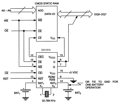
Figure 1. RAM/Time chip interface.
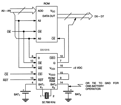
Figure 2. ROM/Time chip interface.
Perhaps the best way to sum up the Dallas Phantom Real-Time Clock family is as follows. The DS1315 Phantom Time Chip is the basic building block that provides timekeeping and a nonvolatile memory controller. The DS1216 then adds a crystal and lithium energy source to the DS1315 and encapsulates them all in a socket that will accept either a RAM or a ROM. Finally, the DS124x modules contain both nonvolatile RAM and timekeeping features in a ready-to-use package.
The entire Dallas Phantom Real-Time Clock family is shown in Table 1.
Table 1.
It should be mentioned that there is some software overhead that is associated with having timekeeping functions that are transparent to RAM as will be discussed in detail below. If it is determined that a transparent clock is not necessary, then the DS164x or DS174x Nonvolatile Timekeeping RAM family could offer an excellent solution to your timekeeping and nonvolatile SRAM needs. These offer nonvolatile SRAM with the Real-Time Clock registers located in the RAM address space. Another possible solution is the DS1386/DS1486 RAMified Watchdog Timekeepers or DS155x Watchdog Timekeeping Family which offer nonvolatile RAM and Real-Time Clock as well as a few extra features including alarm function and Watchdog timer.
The Phantom Real-Time Clock family performs circuit functions required to make a CMOS RAM nonvolatile. First, a switch is provided to direct power from the battery or VCC supply, depending on conditions present. Secondly, When VCC goes out of tolerance, a comparetor outputs a power-fail signal to the chip enable logic. The third function accomplishes write protection by holding the chip enable signal to the memory (active-low CEO) within 0.2 volts of VCC or battery as long as VCC is out of tolerance. During nominal power supply conditions the memory chip enable signal (active-low CEO) will track the chip enable signal (active-low CEO) sent to the socket with a maximum propagation delay of 20 ns.
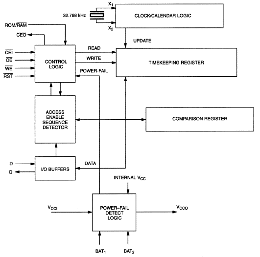
Figure 3. Timing block diagram.
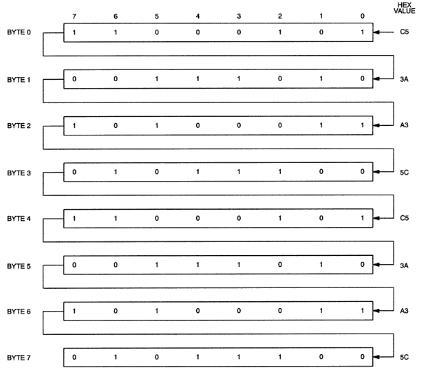
Figure 4. Time chip comparison register definition.
Data transfer to and from the Phantom Clock is accomplished with a serial bit stream under the control of chip enable input (active-low CEI, output enable (active-low OE), and write enable (active-low WE). Initially, a read cycle using the active-low CEI and control of the Phantom Clock starts the pattern recognition sequence by moving a pointer to the first bit of the 64-bit comparison register. Next, 64 consecutive write cycles are executed using the active-low CEI and active-low WE control of the Phantom Clock. These 64 write cycles are used only to gain access to the Phantom Clock. However, the write cycles generated to gain access to the Phantom Clock are also writing data to a location in the mated RAM. The preferred way to manage this requirement is to set aside just one address location in RAM as a scratch pad for the Phantom Clock.
When the first write cycle is executed, it is compared to bit 0 of the 64-bit comparison register. If a match is found, the pointer increments to the next location of the comparison register and awaits the next write cycle. If a match is not found, the pointer does not advance and all subsequent write cycles are ignored until a read cycle is encountered which resets the comparison register pointer to the beginning of the 64-bit comparison register. If a read cycle occurs at any time during the pattern recognition process, the present sequence is aborted and the comparison register pointer is reset. Pattern recognition continues for a total of 64 write cycles as described above until all the bits in the comparison register have been matched (this bit pattern is shown in Figure 4). With a correct match of the 64 bits, the Phantom Clock is enabled and data transfer to or from the timekeeping registers can proceed.
The next 64 cycles will cause the Phantom Clock to either receive or transmit data, depending on the level of the active-low OE pin or the active-low WE pin. Data will either be written to or read from the eight Phantom Clock registers shown in Figure 5. Cycles to other locations outside the memory block can be interleaved with active-low CE cycles without interrupting the pattern recognition sequence or data transfer sequence to the Phantom Clock.
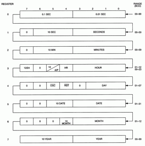
Figure 5. Time chip register definition.
Figure 6 offers an example of pseudo code for both accessing the Phantom Clock embedded in a RAM through pattern recognition and interfacing with the clock registers. Another source code example is given in Figure 7. This code is used for interfacing with the 8051 microcontroller. Also, refer to the data book for timing diagrams for both read and write cycles.
Figure 6. Psuedo Code
Figure 7. Example Source Code for 8051 Microcontroller
In summary, the operation of the Phantom Clocks is best defined as operating in two different modes. The first is the pattern match mode. In this mode, the Phantom Clock is transparent to the system yet monitors communication to the RAM waiting for a match of its 64-bit access pattern. When the 64-bit access pattern has been written, the Phantom Clocks enter the clock access mode. In this mode, the eight phantom clock registers are available to be written or read and will stay in this mode until all eight registers have been accessed, until a reset has been executed, or until a power-fail.
Description
The Dallas Phantom Real Time Clocks are a family of devices that offer the combination of a transparent CMOS timekeeper and a nonvolatile static RAM meeting the standard JEDEC bytewide pinouts. Some varieties of the Dallas Phantom Real Time Clocks also provide a transparent CMOS timekeeper for use with ROM. The timekeeper is transparent to the RAM/ROM memory map because it does not occupy any of the existing RAM/ROM locations. These devices are termed "Phantom" because the timekeeper is accessed only when a predetermined 64-bit pattern has been received by the device. When the timekeeper is not being accessed, the RAM/ROM can be accessed normally. The timekeeper keeps track of hundredths of seconds, seconds, minutes, hours, day, date, month, and year information. In the absence of power, a lithium energy source maintains the timekeeping operation and retains data in the CMOS static RAM.Family Overview
DS1315
The heart of the Dallas Phantom Real-Time Clock family is the DS1315 Phantom Time Chip. This integrated circuit is a combination of a CMOS timekeeper and a nonvolatile memory controller. In the absence of power, an external battery maintains the timekeeping operation and retains data in the CMOS static RAM. The watch keeps track of hundredths of seconds, seconds, minutes, hours, day, date, month, and year information. The last day of the month is automatically adjusted for months with less than 31 days, including correction for leap year every four years. The real-time clock operates in one of two formats: 12-hour mode with an AM/PM indicator or a 24-hour mode. The nonvolatile controller supplies all the necessary support circuitry to convert a CMOS RAM to a nonvolatile memory. The DS1315 can also be used to provide timekeeping functions with ROM.DS1216
Stemming from the DS1315 are the DS1216 SmartWatch Intelligent Sockets. The SmartWatch is a 600-mil wide DIP socket with a built-in DS1315 (providing timekeeping functions and a nonvolatile RAM controller), an embedded lithium energy source, and a 32.768kHz crystal. When the socket is mated with a bytewide CMOS static RAM, it provides a complete solution to problems associated with memory volatility and uses a common energy source to maintain time and date. The DS1216 can also be mated with a ROM to provide timekeeping capability only. Figures 1 and 2 show the basic interface of a SmartWatch with RAM inserted and a SmartWatch with ROM inserted, respectively.
Figure 1. RAM/Time chip interface.

Figure 2. ROM/Time chip interface.
DS1243, DS1244, DS1248, DS1251 and DS1254
The DS124x and DS1254 Nonvolatile SRAM with Phantom Time Clock modules are the members of the Dallas Phantom Real-Time Clock family. These devices are fully nonvolatile static RAM with a built-in Phantom clock, embedded lithium energy source, and 32.768kHz crystal. These devices operate identical to a DS1216 with a RAM inserted. The DS124x Nonvolatile SRAM with Phantom Time Clock modules will maintain over 10 years of data retention in the absence of power.Perhaps the best way to sum up the Dallas Phantom Real-Time Clock family is as follows. The DS1315 Phantom Time Chip is the basic building block that provides timekeeping and a nonvolatile memory controller. The DS1216 then adds a crystal and lithium energy source to the DS1315 and encapsulates them all in a socket that will accept either a RAM or a ROM. Finally, the DS124x modules contain both nonvolatile RAM and timekeeping features in a ready-to-use package.
The entire Dallas Phantom Real-Time Clock family is shown in Table 1.
Table 1.
| DS1315 | Phantom Time Chip |
| DS1216B | SmartWatch/RAM 16k/64k |
| DS1216C | SmartWatch/RAM 64k/256k |
| DS1216D | SmartWatch/RAM 256k |
| DS1216E | SmartWatch/ROM 64k/256k |
| DS1216F | SmartWatch/ROM 64k/256k/1M |
| DS1216H | SmartWatch/RAM 1M/4M |
| DS1243 | 64k NV SRAM with Phantom Clock |
| DS1244 | 256k NV SRAM with Phantom Clock |
| DS1248 | 1024k NV SRAM with Phantom Clock |
| DS1251 | 4M NV SRAM With Phantom Clock |
| DS1254 | 16M NV SRAM With Phantom Clock |
Application
The Dallas Phantom Real-Time Clock family offers two features that will greatly enhance a system. The first feature is nonvolatile RAM capability. The second feature is that the Phantom Clock is transparent to the RAM and therefore timekeeping capacity can be added to a system without changing the existing hardware. All that is required is an existing bytewide memory socket. The retrofit capability is maximized through the transparent interfaces supported by the Phantom Time Chip. Also advantageous to the designer is that an upgrade path is provided to higher RAM densities with the DS124x modules or to higher RAM/ROM densities with the DS1216.It should be mentioned that there is some software overhead that is associated with having timekeeping functions that are transparent to RAM as will be discussed in detail below. If it is determined that a transparent clock is not necessary, then the DS164x or DS174x Nonvolatile Timekeeping RAM family could offer an excellent solution to your timekeeping and nonvolatile SRAM needs. These offer nonvolatile SRAM with the Real-Time Clock registers located in the RAM address space. Another possible solution is the DS1386/DS1486 RAMified Watchdog Timekeepers or DS155x Watchdog Timekeeping Family which offer nonvolatile RAM and Real-Time Clock as well as a few extra features including alarm function and Watchdog timer.
Operation
Nonvolatile RAM Operation
One important feature of the Dallas Phantom Real Time Clocks is that the nonvolatile RAM can be used to store system configuration data and, since the clock is transparent to the RAM, no memory is lost to timekeeping needs. When the Phantom Clock is not accessed, the active-low CE signal is passed on to the chip enable of the memory. Reading and writing to the RAM is identical to that of a standard RAM chip. Figure 1 illustrates a typical RAM/Time Chip interface. Note that this is the basic interface used for the DS1216 SmartWatch/RAM and the DS124x.The Phantom Real-Time Clock family performs circuit functions required to make a CMOS RAM nonvolatile. First, a switch is provided to direct power from the battery or VCC supply, depending on conditions present. Secondly, When VCC goes out of tolerance, a comparetor outputs a power-fail signal to the chip enable logic. The third function accomplishes write protection by holding the chip enable signal to the memory (active-low CEO) within 0.2 volts of VCC or battery as long as VCC is out of tolerance. During nominal power supply conditions the memory chip enable signal (active-low CEO) will track the chip enable signal (active-low CEO) sent to the socket with a maximum propagation delay of 20 ns.
ROM Operation
The DS1315 and DS1216(E/F) can also be used in conjunction with a ROM. A typical ROM/Time Chip interface is illustrated in Figure 2. In this configuration, the ROM/active-low RAM pin is connected to VCCO to select the ROM mode of operation. Since ROM is a read-only device that retains data in the absence of power, battery back-up and write protection is not required. As a result, the chip enable logic will force active-low CEO low when power fails. The real-time clock does retain the same internal nonvolatility and write protection as described in the RAM mode.Real-Time Clock Operation
The block diagram of Figure 3 illustrates the main elements of the Phantom Clock. Communication with the Phantom Clock is established by pattern recognition of a serial bit stream of 64 bits which must be matched by executing 64 consecutive write cycles containing the proper write data as shown in Figure 4. All accesses which occur prior to recognition of the 64-bit pattern are directed to memory via the chip enable output pin (active-low CEO). After recognition is established, the next 64 read or write cycles either extract or update data in the Phantom Clock and active-low CEO remains high during this time, disabling the connected memory.
Figure 3. Timing block diagram.

Figure 4. Time chip comparison register definition.
Note:
The pattern recognition in Hex is C5, 3A, A3, 5C, C5, 3A, A3, 5C. The odds of this pattern being accidentally duplicated and causing inadvertent entry to the Time Chip are less than 1 in 1019. This pattern is sent to the Phantom Clock LSB to MSB.Data transfer to and from the Phantom Clock is accomplished with a serial bit stream under the control of chip enable input (active-low CEI, output enable (active-low OE), and write enable (active-low WE). Initially, a read cycle using the active-low CEI and control of the Phantom Clock starts the pattern recognition sequence by moving a pointer to the first bit of the 64-bit comparison register. Next, 64 consecutive write cycles are executed using the active-low CEI and active-low WE control of the Phantom Clock. These 64 write cycles are used only to gain access to the Phantom Clock. However, the write cycles generated to gain access to the Phantom Clock are also writing data to a location in the mated RAM. The preferred way to manage this requirement is to set aside just one address location in RAM as a scratch pad for the Phantom Clock.
When the first write cycle is executed, it is compared to bit 0 of the 64-bit comparison register. If a match is found, the pointer increments to the next location of the comparison register and awaits the next write cycle. If a match is not found, the pointer does not advance and all subsequent write cycles are ignored until a read cycle is encountered which resets the comparison register pointer to the beginning of the 64-bit comparison register. If a read cycle occurs at any time during the pattern recognition process, the present sequence is aborted and the comparison register pointer is reset. Pattern recognition continues for a total of 64 write cycles as described above until all the bits in the comparison register have been matched (this bit pattern is shown in Figure 4). With a correct match of the 64 bits, the Phantom Clock is enabled and data transfer to or from the timekeeping registers can proceed.
The next 64 cycles will cause the Phantom Clock to either receive or transmit data, depending on the level of the active-low OE pin or the active-low WE pin. Data will either be written to or read from the eight Phantom Clock registers shown in Figure 5. Cycles to other locations outside the memory block can be interleaved with active-low CE cycles without interrupting the pattern recognition sequence or data transfer sequence to the Phantom Clock.

Figure 5. Time chip register definition.
Figure 6 offers an example of pseudo code for both accessing the Phantom Clock embedded in a RAM through pattern recognition and interfacing with the clock registers. Another source code example is given in Figure 7. This code is used for interfacing with the 8051 microcontroller. Also, refer to the data book for timing diagrams for both read and write cycles.
* This code will access the Phantom Time Clock by sending the 64-bit   *
* access pattern.  Then the time data will be written to the clock and *
* finally the Phantom Time Clock will be accessed again and it will be *
* read. The time information to be written is 12:00 PM Wednesday,      *
* January 1, 1992. Also note that the oscillator has been enabled and  *
* reset has been disabled.                                             *

A : Array[0..7] = (C5, 3A, A3, 5C, C5, 3A, A3, 5C)    (access pattern)
T : Array[0..7] = (00, 00, 00, B2, 14, 01, 01, 92)    (time data)
X : Byte at 1000                       (memory location 1000H)
D : Array [0..7]
S : Byte

* Send access pattern to Phantom Time Clock *
FOR I = 0 TO 64 S = x                  (perform 65 consecutive reads from x)
FOR I = 0 TO 7                         (loop for 8 bytes)
FOR J = 0 TO 7                         (loop for 8 bits)
X = A[I] SHR J                         (write to X, shift bits right J)
NEXT J
NEXT I

* Write time data to Phantom Time Clock registers *
FOR I = 0 TO 7                         (loop for 8 bytes)
FOR J = 0 TO 7                         (loop for 8 bits)
X = T[I] SHR J                         (write to X, shift bits right J)
NEXT J

* Send access pattern to Phantom Time Clock *
FOR I = 0 TO 64 S = X                  (perform 65 consecutive reads from X)
FOR I = 0 TO 7                         (loop for 8 bytes)
FOR J = 0 TO 7                         (loop for 8 bits)
X = A[I] SHR J
NEXT J
NEXT I

* Read Phantom Time Clock registers *
FOR I = 0 TO 7                         (loop for 8 bytes)
D[I] = 0                               (initiate the byte)
FOR J = 0 TO 7                         (loop for 8 bits)
D[I] = D[I] or (X and 1) SHL J         (position bits in byte)
NEXT J
NEXT I
Figure 6. Psuedo Code
; 8051CODE.DOC
; RTC procedure to access the DS1215 Serial Timekeeper, or DS1216
; SmartWatch using 8031, 8051 or 80C196
;
BIT_SEG SEGMENT BIT
RSEG  BITSEG
WF:   DBIT  1
BYTE_SEG       SEGMENT DATA
RSEG  BYTE_SEG
BUFF:    DS       8  ;Centi-sec: 00-99
;                    ;Seconds: 00-59
;                    ;Minutes: 00-59
;                    ;Hours: 01-12 / 00-23
;                    ;Day:1nHEX % RST off, n=DAY# 01-07
;                    ;Date: 01-31
;                    ;Month: 01-12
;                    ;Year: 00-99
CODESEG SEGMENT CODE
RSEG  CODE_SEG
;**************************
;*** MAIN PROGRAM GOES HERE
;**************************
;
; Main program SETS WF for Read Mode and on return from RTC the BUFF will
; contain the 8 bytes of data read from the clock.  If WF is CLEARED then
; RTC will return after writing the 8 byte BUFF to the clock.
;
;  NOTE !!! : Refer to the DS1215 (RAM MODE) or DS1216 data sheet.
;
RTC:     PUSH PSW           ;Save user registers.
PUSH     ACC
PUSH     B
MOV      B, RO
PUSH     B
MOV      RO, #BUFF          ;Load pointer to start of table.
LCALL    OPEN               ;Set up to open the DS1216.
MOV      B, #8H             ;Load loop counter for 8 bytes.
JNB      WF, WRITETIME      ;Read/Write mode check.
;
READTIME: LCALL RBYTE       ;Read one byte.
MOV      @RO, A             ;Save in RTn temporary register.
INC      R0                 ;Temporary data register pointer.
DJNZ     B, READTIME        ;Loop to read 8 bytes.
SJMP     ENDTIME            ;Done reading goto finish.
;
WRITETIME: MOV A, @R0       ;Load byte of data to be written.
LCALL    WBYTE              ;Write one byte.
INC      R0                 ;Temporary data register pointer.
DJNZ     B, WRITETIME       ;Loop to write 8 bytes.
;
ENDTIME: POP B              ;Restore registers.
MOV      R0, B
POP      B
POP      ACC
POP      PSW
RET                         ;Return to main calling program.
;
;
;
;
;**************************************
; SUBROUTINE TO OPEN THE CLOCK/CALENDAR
;**************************************
;
; This subroutine executes the sequence of reads and writes which
; is required in order to open communication with the timekeeper.
;
OPEN:    LCALL CLOSE        ;Make sure it is closed.
MOV      B, #4              ;Set pattern period count.
MOV      A, #0C5H           ;Load first byte of pattern.
OPENA:   LCALL WBYTE        ;Send out the byte.
XRL      A, #0FFH           ;Generate next pattern byte.
LCALL    WBYTE              ;Send out the byte.
SWAP     A                  ;Generate next pattern byte.
DJNZ     B, OPENA           ;Repeat until 8 bytes sent.
RET                         ;Return.
;
;******************************
;*** SUBROUTINE TO CLOSE CLOCK
;******************************
;
; This subroutine insures that the registers of the timekeeper
; are closed by executing 72 successive reads of the date and time
; registers.
;
CLOSE:   MOV B, #9          ;Set up to read 9 bytes.
CLOSEA:  LCALL RBYTE        ;Read a byte.
DJNZ     B, CLOSEA          ;Loop for 9 byte reads.
RET                         ;Return
;
;***********************************
:*** SUBROUTINE TO READ A DATA BYTE
;***********************************
;
RBYTE:   PUSH DPL           ;Save the data
PUSH     DPH                ;pointer on stack.
PUSH     B                  ;Save the B register.
MOV      DPTR, #RTCADDR     ;Enable the clock.
MOV      B, #8              ;Set the bit count.
LI:      PUSH ACC           ;Save the accumulator.
MOVX     A, @DPTR           ;Input the data bit.
RRC      A                  ;Move it to carry.
POP      ACC                ;Get the accumulator.
RRC      A                  ;Save the data bit.
DJNZ     B, LI              ;Loop for a whole byte.
POP      B                  ;Restore the B register.
POP      DPH                ;Restore the data
POP      DPL                ;pointer from stack.
RET                         ;Return.
;
;
;
;***********************************
;*** SUBROUTINE TO WRITE A DATA BYTE
;***********************************
;
WBYTE:   PUSH DPL           ;Save the data
PUSH     DPH                ;pointer on stack.
PUSH     B                  ;Save the B register.
MOV      DPTR, #RTCADDR     ;Enable the clock.
MOV      B, #8              ;Set the bit count.
L      PUSH ACC           ;Save the accumulator.
ANL      A, #1              ;Set up bit for output.
MOVX     @DPTR, A           ;Output the data bit.
POP      ACC                ;Restore the accumulator.
RR       A                  ;Position next bit.
DJNZ     B, LO              ;Loop for a whole byte.
POP      B                  ;Restore the B register.
POP      DPH                ;Restore the data
POP      DPL                ;pointer from stack.
RET                         ;Return.
;
;***************
;END OF PROGRAM
;***************
;
END                        ;End of program.
Figure 7. Example Source Code for 8051 Microcontroller
In summary, the operation of the Phantom Clocks is best defined as operating in two different modes. The first is the pattern match mode. In this mode, the Phantom Clock is transparent to the system yet monitors communication to the RAM waiting for a match of its 64-bit access pattern. When the 64-bit access pattern has been written, the Phantom Clocks enter the clock access mode. In this mode, the eight phantom clock registers are available to be written or read and will stay in this mode until all eight registers have been accessed, until a reset has been executed, or until a power-fail.
Troubleshooting
The Dallas Phantom Real Time Clocks have proven to be highly reliable and meet the published specifications. However, in the course of development, several common difficulties could be experienced. To reduce these difficulties, Dallas Semiconductor has gathered the common difficulties and pitfalls into a troubleshooting guide to assist users.Common Difficulties
Cannot Access Clock Registers
Several items can cause this phenomenon.- Comparison register pointer has not been set to the first bit. The Phantom Real-Time Clock hides behind the SRAM and waits for a match to its 64-bit access pattern. In this mode (the pattern match mode), every write operation to the RAM will be interpreted as an attempt to match the access pattern by matching the value written to DQ0 (D for the DS1315) to the pattern bit pointed to by the pattern match pointer. It is possible that a partial match of the pattern can occur during normal operation of a system. It is best to assume that there is a partial match of the access pattern and that the comparison register pointer is not pointing to the first bit of the match pattern. Therefore, the comparison register pointer must be reset to the first pattern bit before writing the match pattern. This is accomplished by performing one read operation of the RAM before writing the match pattern.
- Device is in clock access mode after system reset or interrupt. It is possible that during the course of previous operation, the Phantom Clock had been accessed, but had not gone back into pattern match mode before a system reset or interrupt occurred. In other words, data bits would be written to or read from the Phantom Clock registers rather than the RAM. A solution to this problem is to execute 65 consecutive read cycles immediately after an interrupt or system reset. This will insure that the device is taken out of the clock access mode (by reading a maximum of 64 bits) and will reset the comparison register pointer.
- Access pattern has been input in reverse order. Insure that the pattern is input in the following order. Start with bit 0 of byte 0 continuing to bit 7 of byte 7.
- Device is being reset. Insure that the device is not accidentally being reset. This can especially be a problem with the DS1216C, DS1216D, DS1216H, DS1244 and DS1251 where the reset pin is shared with an address pin. In this situation, that particular address line must never be taken low unless the reset bit (byte 4, bit 4) of the Phantom Clock is disabled, otherwise the device will be reset and the data transfer will be aborted.
- Device is in constant write protect mode. If only one battery is being used for the DS1315, ensure that the BAT2 pin is grounded. If this pin remains floating it is possible that the device will not switch to the battery during power fail.
Device Will Not Oscillate
- Oscillator enable bit is disabled. Insure that the oscillator enable bit (bit 5 of byte 4) is at logic 0.
- Wrong crystal used (DS1315). Insure that the correct crystal is being used. It is very important that a crystal with a load capacitance of 6pF is used. Dallas Semiconductor recommends Seiko part number DS-VT-200, Daiwa part number DT-26S, or equivalent.
- Poor crystal connection (DS1315). To insure the greatest performance, insure that the crystal is placed as close as possible to the crystal input pins. It should also be mentioned that the DS1315 does not require load capacitors or feedback resistors.
Note:
It should also be mentioned that attempting to monitor the oscillator at the crystal connections may cause the oscillator to stop due to excess capacitance and/or leakage current added by the scope probe.Timekeeping Inaccurate
- Wrong crystal used (DS1315). For best accuracy, insure that the correct crystal is used.
- Input pins driven higher than VCC. It is very important to insure that input pins never go above VCC. If any input is allowed to go above VCC, it is possible that the oscillator may be briefly stopped, which will cause the device to lose time.
- Fast Clock: The crystal oscillator is sensitive to high levels of EMI which will cause the clock to run fast. Locating the unit next to a microprocessor, chopper power supply, on top of high speed data or Address lines or high EMI sources is not recommended. The EMI interference test for a fast clock is to shield the part with copper shielding or metal tape connected to ground and determine the clock accuracy with the shield in place.
- Slow Clock: If undershoots greater than 0.6 volts are present on any pin to a RTC then the clock could run slow. This is because the oscillator can miss a count during the undershoot. The design should be modified to incorporate Schottky diodes on all pins with undershoots.
- RAM is loosing Data During Power-down Sequence: This problem can occur especially in NMOS processors which become unstable at a higher voltage than CMOS processors. Write protection is asserted when VCC drops below VpF, Therefore, in a power-down situation, if the processor becomes unstable at a VCC of greater than VpF (which is often the case for an NMOS processor), a spurious write cycle could corrupt the data in the Phantom Clock. The solution to this problem is to ensure that the processor is reset before it becomes unstable and thus prevent any unwanted writes from being executed. This can be accomplished by monitoring VCC by one of Dallas Semiconductor's power monitors (the DS123x family) which generate a reset signal when VCC is out of tolerance.
- Another known cause of data disturb is undershoot of the VCC voltage during power up or power down events. This situation can be caused by some types of power supplies and should be avoided. The cure for this problem is to add a Schottky diode to the VCC pin in order to clamp the negative undershoots. In addition of a by pass cap at the device VCC and ground pins may also help.
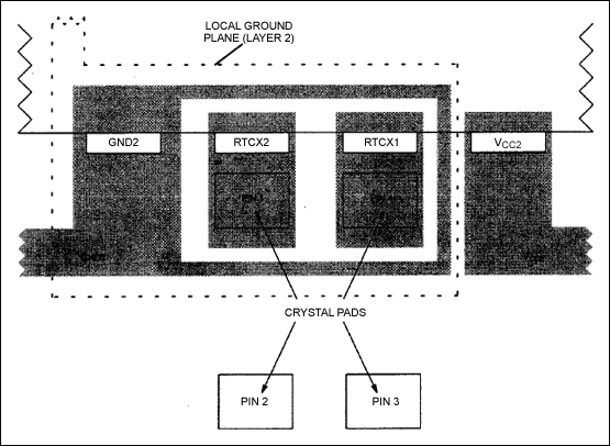
- Cross-talk and EMI considerations: Caution should be taken in the design layout for all RTC's to avoid cross-talk and EMI effects to the sensitive clock oscillator circuits. Clock, Data and Address lines should not be located underneath the crystal when using a discrete component or directly underneath a module or PowerCap system. The addition of ground metal underneath the device will enhance the EMI and cross-talk rejection into the a RTC system. Decoupling of lower order addresses and other fast rise time inputs will also eliminate interference with the clock accuracy due to cross-talk. Locating an RTC in the vicinity of a strong EMI source such as a switching power supply or transformer. For additional information on crystal location and system design considerations see Application Note 58
Cannot Read Consecutive Hundredths of Seconds
It is not possible to read consecutive hundredths of seconds because the access time to read the clock registers is too long.Common Pitfalls
- Device needs separate read and write signals. The Dallas Phantom Real Time Clocks were designed with Intel timing in mind. Therefore it is necessary to have separate read and write signals. It should be further stressed that simply complementing one signal to arrive at the other is not sufficient because this will cause the pattern match pointer to be reset during each write cycle since the active-low OE signal will toggle whenever the active-low WE signal toggles.
- Battery attachment (DS1315). Any battery attached to the BAT1 or BAT2 pins must be connected directly to the pin. It should be noted that a diode should not be connected between the battery input pin and the battery. This is not necessary because internal reverse charging current protection circuitry is provided and is UL recognized (#E99151).
- ROM/active-low RAM pin (DS1315). Insure that the ROM/RAM pin is set to the correct value.
- Reading and writing to clock registers. It is important that all 64 bits be read or written to when the clock registers have been accessed. If this is not done, the device will remain in the clock access mode.
- Do not water wash DS1216 Intelligent Sockets. Water washing for flux removal must not be performed on the DS1216 Intelligent Sockets because contaminants in the water can cause discharging of the internal lithium energy source.
- Crystal selection (DS1315). A 32.768kHz quartz crystal, Seiko part number DS-VT-200, Daiwa part number DT-26S, or equivalent should be used. The crystal selected for use must have a specified load capacitance of 6pF. The use of an incorrect crystal can kill the oscillator or cause accuracy problems. Also, the use of an external trim capacitor to adjust the oscillator is discouraged.
 電子發燒友App










評論