Introduction
The DS89C430 high-speed microcontroller's serial interface is functionally identical to those found on other 8051 processors.This application note describes the setup and operation of the most commonly encountered operating mode of this interface, 10-bit asynchronous or standard full-duplex asynchronous communication mode 1. A general overview of the port's operation, especially mode 1 operation and baud-rate generation, will be provided. Detailed software examples will be presented. Examples illustrate the use of dual serial ports with different timer configurations. The DS89C430 User's Guide and Appendix A below describe all the DS89C430 registers involved in system clock-frequency settings, baud-rate generation, and serial-port operations.
Baud-Rate Generation
Each mode has a baud-rate generator associated with it. This generator is generally the same for each UART. Several of the baud-rate generation techniques have options that are independent for the two UARTs. The following baud-rate descriptions are specific to the timer used and baud-rate-generation formula for a serial port configured for mode 1 operation.Using Timer 1 for Baud-Rate Generation
To use timer 1 as the baud-rate generator, it is commonly put into the 8-bit autoreload mode. In this way, the CPU is not involved in baud-rate generation. Note that the timer interrupt should not be enabled. In the 8-bit autoreload mode (timer 1, mode 2), the reload value is stored in TH1. Thus, the combination of timer 1 input-clock frequency and TH1 determine the baud rate. The timer 1 input clock, relative to the external crystal clock, can be altered in two ways:- Change the system clock, or
- Change the timer input clock divide ratio.
Table 1 summarizes the relationship between the external crystal frequency and the timer 1 input clock for each of the various configurations.
Table 1. Timer 1 Input-Clock Frequency
| System Clock Mode | PMR Register Bits (4x/2x, CD1, CD0) |
Timer 1 Input-Clock Frequency | ||
| T1MH, T1M = 00 | T1MH, T1M = 01 | T1MH, T1M = 1X | ||
| Crystal Multiply Mode 4X | 100 | OSC/12 | OSC/1 | OSC/0.25 |
| Crystal Multiply Mode 2X | 000 | OSC/12 | OSC/2 | OSC/0.5 |
| Divide-by-1 (default) | X01, X10 | OSC/12 | OSC/4 | OSC/1 |
| Power-Management Mode (/1024) | X11 | OSC/3072 | OSC/1024 | OSC/1024 |
Baud-Rate Formula Using Timer 1
Table 2 lists reload values for the TH1 register for generating some of the more common baud rates.
Table 2. Mode 1 Baud Rates—Timer 1 Reload Values
| Baud Rate | SMOD | Input-Clock Frequency (Divide-by-1) | |
| TH1—Reload Value | |||
| OSC = 11.05MHz | OSC = 22.11MHz | ||
| 115200 | 0/1 | FD/FA | FA/F4 |
| 57600 | 0/1 | FA/F4 | F4/E8 |
| 38400 | 0/1 | F7/EE | EE/DC |
| 28800 | 0/1 | F4/E8 | E8/D0 |
| 19200 | 0/1 | EE/DC | DC/B8 |
| 14400 | 0/1 | E8/D0 | D0/A0 |
| 9600 | 0/1 | DC/B8 | B8/70 |
| 1200 | 0/1 | N/A | N/A |
Using Timer 2 for Baud-Rate Generation
To use timer 2 as the baud-rate generator for serial port 0, the timer is configured in autoreload mode. Then, either the TCLK or RCLK bit (or both) are set to a logic 1. TCLK = 1 selects timer 2 as the baud-rate generator for the transmitter; RCLK = 1 selects timer 2 for the receiver. Thus, serial port 0 can have the transmitter and receiver operating at different baud rates by choosing timer 1 for one data direction and timer 2 for the other. RCLK and TCLK reside in T2CON.4 and TCON.5, respectively.Although the timer 2 input clock can be configured similarly to timer 1, it must be placed into a baud-rate generator mode to be used by serial port 0. Setting either RCLK or TCLK to a logic 1 selects timer 2 for baud-rate generation. When this is done, the timer 2 input clock becomes fixed to the oscillator frequency divided by 2. The only exception is when timer 2 is used for baud-rate generation within power-management mode (PMM). For PMM, the system clock (OSC/1024) is used as the input clock for timer 2. The timer 2 interrupt is automatically disabled when either RCLK or TCLK is set. Also, the TF2 (TCON.7) flag is not set on a timer rollover. The following Table 3 summarizes the relationship between the external crystal frequency and the timer 2 input clock for the various configurations.
Table 3. Timer 2 Input-Clock Frequency
| System Clock Mode | PMR Register Bits (4x/2x, CD1, CD0) |
Timer 2 Input-Clock Frequency Baud-Rate Generator Mode (RCLK or TCLK = 1) |
| Crystal Multiply Mode 4X | 100 | OSC/2 |
| Crystal Multiply Mode 2X | 000 | OSC/2 |
| Divide-by-1 (default) | X01, X10 | OSC/2 |
| Power-Management Mode (/1024) | X11 | OSC/1024 |
Baud-Rate Formula Using Timer 2
Table 4 shows reload values for the RCAP2H and RCAP2L registers for generating some of the more common baud rates.
Table 4. Mode 1 Baud Rates—Timer 2 Reload Values
| Baud Rate | Input-Clock Frequency (Divide-by-1) | |
| RCAP2H/RCAP2L—Reload Value | ||
| OSC = 11.05MHz | OSC = 22.11MHz | |
| 115200 | FF/FD | FF/FA |
| 57600 | FF/FA | FF/F4 |
| 38400 | FF/F7 | FF/EE |
| 28800 | FF/F4 | FF/E8 |
| 19200 | FF/EE | FF/DC |
| 14400 | FF/E8 | FF/D0 |
| 9600 | FF/DC | FF/B8 |
| 1200 | FE/E0 | FD/C0 |
Serial-Port Initialization
To use the UART function (s), the serial port must be initialized. This process involves selecting the mode and time base, then initializing the baud-rate generator. Serial communication is then available. See Table 5. Once the baud-rate generator is running, the UART can transmit/receive data. Most of the serial-port controls are provided by the SCON0 and SCON1 registers. For detailed bit descriptions of these registers, please refer to the DS89C430 User's Guide cited above.Table 5. Serial-Ports Mode Functions
| SM0 | SM1 | SM2 | Mode | Function | Length (Bits) | Period |
| 0 | 0 | 0 | 0 | Synchronous | 8 | See PMR register |
| 0 | 0 | 1 | 0 | Synchronous | 8 | See PMR register |
| 0 | 1 | X | 1 | Asynchronous | 10 | Timer 1 or 2 (port 0 only) baud rate equation |
| 1 | 0 | 0 | 2 | Asynchronous | 11 | See PMR register |
| 1 | 0 | 1 | 2 | Asynchronous with multiprocessor communication | 11 | See PMR register |
| 1 | 1 | 0 | 3 | Asynchronous | 11 | Timer 1 or 2 (port 0 only) baud rate equation |
| 1 | 1 | 1 | 3 | Asynchronous with multiprocessor communication | 11 | Timer 1 or 2 (port 0 only) baud rate equation |
Mode 1
As mentioned earlier, we are only interested in asynchronous mode 1 operation. This asynchronous mode is commonly used for communication with PCs, modems, and other similar interfaces. This mode provides standard full-duplex asynchronous communication. A total of 10 bits are transmitted including 1 start bit, 8 data bits, and 1 stop bit. The received stop bit is stored in bit location RB8 of the relevant SCON register.In mode 1, the baud rate is a function of timer overflow. This makes the baud rate programmable by the user. One difference that exists between the two UARTs with respect to mode 1 configuration: serial port 1 can use only timer 1. In contrast, serial port 0 can use either timer 1 or timer 2 to generate baud rates. If both serial ports use the same timer, they run at the same baud rate. Alternatively, one timer can run twice as fast as the other (when baud-rate doubler bits, PCON.7 and WDCON.7, are configured differently). If the two UARTs use different timers, the baud-rate configurations in relation to one another are not as restrictive. Baud-rate generation for mode 1 is discussed above in the Baud Rate Generation section for both timer 1 and timer 2. The following examples provide more details.
Serial Communication Interrupts
Each UART can generate an interrupt, and each UART has its own interrupt enable, vector, and priority. Each UART interrupt has two flags (RI, TI) used by the ISR to determine whether the interrupt comes from a received word or a transmitted one. When a UART finishes the transmission of a word, the TI bit is set and an interrupt is generated (if enabled). Likewise, the UART sets the RI bit and generates an interrupt when a word is received completely. The CPU is not notified until the word is completely received or transmitted. Alternatively, if the interrupts are enabled, the setting of either of these flags causes a jump to the serial channel's associated interrupt vector. The interrupt vector table for the DS89C430 is provided in Table 6.Table 6. DS89C430 Interrupt Vector
| Interrupt | Interrupt Vector | Natural Order | Interrupt Flag | Enable | Priority Control |
| Power-fail | 0033h | 0 (highest) | PFI (WDCON.4) | EPFI (WDCON.5) | N/A |
| External Interrupt 0 | 0003h | 1 | IE0 (TCON.1) | EX0 (IE.0) | MPX0 (IP1.0)/LPX0 (IP0.0) |
| Timer 0 Overflow | 000Bh | 2 | TF0 (TCON.5) | ET0 (IE.1) | MPT0 (IP1.1)/LPT0 (IP0.1) |
| External Interrupt 1 | 0013h | 3 | IE1 (TCON.3) | EX1 (IE.2) | MPX1 (IP1.2)/LPX1 (IP0.2) |
| Timer 1 Overflow | 001Bh | 4 | TF1 (TCON.7) | ET1 (IE.3) | MPT1 (IP1.3)/LPT1 (IP0.3) |
| Serial Port 0 | 0023h | 5 | RI_0 (SCON0.0)/TI_0 (SCON0.1) | ES0 (IE.4) | MPS0 (IP1.4)/LPS0 (IP0.4) |
| Timer 2 Overflow | 002Bh | 6 | TF2 (T2CON.7)/EXF2 (T2CON.6) | ET2 (IE.5) | MPT2 (IP1.5)/LPT2 (IP0.5) |
| Serial Port 1 | 003Bh | 7 | RI_1 (SCON1.0)/TI_1 (SCON1.1) | ES1 (IE.6) | MPS1 (IP1.6)/LPS1 (IP0.6) |
| External Interrupt 2 | 0043h | 8 | IE2 (EXIF.4) | EX2 (EIE.0) | MPX2 (EIP1.0)/LPX2 (EIP0.0) |
| External Interrupt 3 | 004Bh | 9 | IE3 (EXIF.5) | EX3 (EIE.1) | MPX3 (EIP1.1)/LPX3 (EIP0.1) |
| External Interrupt 4 | 0053h | 10 | IE4 (EXIF.6) | EX4 (EIE.2) | MPX4 (EIP1.2)/LPX4 (EIP0.2) |
| External Interrupt 5 | 005Bh | 11 | IE5 (EXIF.7) | EX5 (EIE.3) | MPX5 (EIP1.3)/LPX5 (EIP0.3) |
| Watchdog Interrupt | 0063h | 12 | WDIF (WDCON.3) | EWDI (EIE.4) | MPWDI (EIP1.4)/LPWDI (EIP0.4) |
To develop C code using the Keil? compiler, we need to match the interrupt vector of the DS89C430 with its interrupt number. Table 7 shows the Keil C compiler numbers for the interrupts.
Table 7. Keil Interrupts for the DS89C430
| Interrupt Number | Address | Interrupt Number | Address |
| 0 (External Interrupt 0) | 0003h | 16 | 0083h |
| 1 (Timer/Counter 0) | 000Bh | 17 | 008Bh |
| 2 (External Interrupt 1) | 0013h | 18 | 0093h |
| 3 (Timer/Counter 1) | 001Bh | 19 | 009Bh |
| 4 (Serial Port) | 0023h | 20 | 00A3h |
| 5 (Timer/Counter 2) | 002Bh | 21 | 00ABh |
| 6 | 0033h | 22 | 00B3h |
| 7 | 003Bh | 23 | 00BBh |
| 8 | 0043h | 24 | 00C3h |
| 9 | 004Bh | 25 | 00CBh |
| 10 | 0053h | 26 | 00D3h |
| 11 | 005Bh | 27 | 00DBh |
| 12 | 0063h | 28 | 00E3h |
| 13 | 006Bh | 29 | 00EBh |
| 14 | 0073h | 30 | 00F3h |
| 15 | 007Bh | 31 | 00FBh |
From Table 7, serial port 0 is assigned interrupt number 4 and serial port 1 is assigned interrupt number 7.
Creating and Compiling the C Application with the Keil C Compiler
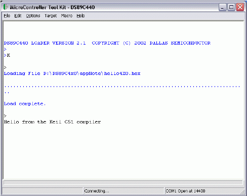
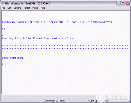
It is assumed that the reader already has the Keil C compiler. Please refer to application note 3267, "Using the Keil C Compiler with the DS89C430/450." This application note explains how to use the Keil μVision? suite of tools to build a C application for Maxim's ultra-high-speed family of flash microcontrollers, which includes the DS89C430. The process of loading the compiled application into the microcontroller using Maxim's Microcontroller Tool Kit (MTK) application is also covered. The DS89C430 is socketed into the DS89C450 evaluation (EV) kit. For the setup and positions of the DIP switches of this board, please review the full DS89C450 data sheet. To use serial port 1, please place SW1.6 and SW1.7 in the ON positions.Dual Serial-Port Examples
The following examples demonstrate the use of the two serial ports available on the DS89C430. They illustrate how to initialize and use both serial ports at different baud rates generated by different timers. As discussed earlier, much of the information regarding serial port 0 applies equally to serial port 1. However, these examples will help clarify any confusion about using the serial ports.In all the examples, the software simply outputs a message to a terminal application (MTK shown here) connected to both port 0 and port 1, respectively. The software then waits for input. When either terminal sends a character to the DS89C430, the associated RI bit is set. An interrupt lets the software recognize that this bit has been set. The software then reads the received character and transfers it to the transmit buffer of both serial ports. For illustrative purposes, the character is echoed back to terminal 0 through serial port 0 and increased by 1 before being transferred to terminal 1 through serial port 1.
In the examples, the input clock frequency is set to the default of divide-by-1; the two SMOD bits are cleared; the timers' interrupts are disabled; the timers' modes are initialized; and the count and reload registers are loaded. This completely configures the baud clock generation. After the two serial control registers are set for the desired modes, the timers are started and serial communication begins. All software application examples include the DualPort.h header file that contains the interrupt subroutines and other utility functions. The contents of this file are listed in Appendix B.
Example 1
In this example, both serial ports are set to run from a baud clock generated from timer 1 at 9600bps.#includevoid main () { /* Need to set system clock as default because the system - see note 1*/ initSystem (); /* Set up Timer1 */ initTimer1 (BR9600); /* Set up Timer2 */ //initTimer2 (0x30, BR9600, 0xff); /* Set up serial port 0 & 1 and their interrupts*/ initSerialPorts (); /* Send "Hello" banner for each serial port */ WriteBanner0 (); WriteBanner1 (); /* Send data to any serial port and get echo back from port 0 and +1 for port 1 */ while (1) { if (RI || RI1) { SerialTX0 (RxTxChar); SerialTX1 (RxTxChar+1); } } }
Example 2
In this example both serial ports are set to run from a baud clock generated from timer 1. Serial port 0 doubles the baud rate and runs at 28800bps, compared to serial port 1 running at 14400bps.#includevoid main () { /* Need to set system clock as default because the system - see note 1*/ initSystem (); /* Set up Timer1 */ initTimer1 (BR14400); PCON = 0x80; // Set SMOD_0 /* Set up Timer2 */ //initTimer2 (0x30, BR9600, 0xff); /* Set up serial port 0 & 1 and their interrupts*/ initSerialPorts (); /* Send "Hello" banner for each serial port */ WriteBanner0 (); WriteBanner1 (); /* Send data to any serial port and get echo back from port 0 and +1 for port 1 */ while (1) { if (RI || RI1) { SerialTX0 (RxTxChar); SerialTX1 (RxTxChar+1); } } }
Example 3
In this example both serial ports are set to run from a baud clock generated from timer 1. Serial port 1 doubles the baud rate and runs at 19200bps, compared to serial port 0 running at 9600bps.#includevoid main () { /* Need to set system clock as default because the system - see note 1 */ initSystem (); /* Set up Timer1 */ initTimer1 (BR9600); WDCON = 0x80; // Set SMOD_1 /* Set up Timer2 */ //initTimer2 (0x30, BR9600, 0xff); /* Set up serial port 0 & 1 and their interrupts*/ initSerialPorts (); /* Send "Hello" banner for each serial port */ WriteBanner0 (); WriteBanner1 (); /* Send data to any serial port and get echo back from port 0 and +1 for port 1 */ while (1) { if (RI || RI1) { SerialTX0 (RxTxChar); SerialTX1 (RxTxChar+1); } } }
Example 4
In this example, serial port 1 is set to run from a baud clock generated from timer 1 at 57600bps. Serial port 0 uses timer 2 to run at 115200bps.#includevoid main () { /* Need to set system clock as default because the system - see note 1*/ initSystem (); /* Set up Timer1 */ initTimer1 (BR57600); /* Set up Timer2 */ initTimer2 (0x30, BR115200, 0xff); /* Set up serial port 0 & 1 and their interrupts*/ initSerialPorts (); /* Run timers to generate baud rate */ /* Send "Hello" banner for each serial port */ WriteBanner0 (); WriteBanner1 (); /* Send data to any serial port and get echo back from port 0 and +1 for port 1 */ while (1) { if (RI || RI1) { SerialTX0 (RxTxChar); SerialTX1 (RxTxChar+1); } } }
Example 5
In this example serial port 1 is set to run from a baud clock generated from timer 1 at 9600bps. Serial port 0 uses both timers: timer 1 at 9600bps for receiving, and timer 2 at 19200bps for transmitting.#includevoid main () { /* Need to set system clock as default because the system - see note 1*/ initSystem (); /* Set up Timer1 */ initTimer1 (BR9600); /* Set up Timer2 */ initTimer2 (0x10, BR19200, 0xff); /* Set up serial port 0 & 1 and their interrupts*/ initSerialPorts (); /* Send "Hello" banner for each serial port */ WriteBanner0 (); WriteBanner1 (); /* Send data to any serial port and get echo back from port 0 and +1 for port 1 */ while (1) { if (RI || RI1) { SerialTX0 (RxTxChar); SerialTX1 (RxTxChar+1); } } }
Example 6
In this example serial port 1 is set to run from a baud clock generated from timer 1 at 14400bps. Serial port 0 uses both timers: timer 1 at 14400bps for transmission, and timer 2 at 57600bps for receiving.#includeNote 1*: Creating, compiling, and loading a new project in the Keil C compiler may require the startup code file named START4XX.A51. This file is part of the C51 Compiler package and is executed after processor reset. The user can add this file to the project, but it may change the system clock frequency if the assembly constant CLOCKADJUST is set to 1. The initSystem () procedure is used to ensure that the system clock frequency is set to divide-by-1, as expected.void main () { /* Need to set system clock as default because the system - see note 1*/ initSystem (); /* Set up Timer1 */ initTimer1 (BR14400); /* Set up Timer2 */ initTimer2 (0x20, BR57600, 0xff); /* Set up serial port 0 & 1 and their interrupts*/ initSerialPorts (); /* Send "Hello" banner for each serial port */ WriteBanner0 (); WriteBanner1 (); /* Send data to any serial port and get echo back from port 0 and +1 for port 1 */ while (1) { if (RI || RI1) { SerialTX0 (RxTxChar); SerialTX1 (RxTxChar+1); } } }
Conclusions
This application note shows how easy it is to implement a 10-bit asynchronous UART in software using two standard serial ports. The same techniques can be used to implement any serial port in the ultra-high-speed flash family of microcontrollers, which includes the DS89C430, the DS89C450, or other high-speed 8051-compatible devices. The clock multiplier and selectable high-speed clock of the timers can directly affect baud rate generation for the serial ports. Users can set serial-port baud rates that are directly derived from the speed of selected timers. For the baud rate formula of different serial-port modes, please refer to the DS89C430 User's Guide.Appendix A
System Registers
Power Management Register (PMR)CD1, CD0 (Bits 7, 6)
Clock Divide Control 1-0: These bits select the number of crystal oscillator clocks required to generate one machine cycle. Switching between modes requires a transition through the default divide-by-1 mode (CD1, CD0 = 10b). Attempts to perform an invalid transition are ignored. For example, going from the crystal multiplier 2X mode to the divide-by-1024 mode would require first switching from the 2X crystal multiplier mode to the divide-by-1 mode, followed by the switch from the divide-by-1 to the divide-by-1024 mode. These bits cannot be modified when running from the internal ring oscillator (RGMD = 1). The divide-by-1024 setting (CD1, CD0 = 11b) cannot be selected when switchback is enabled (SWB = 1) and a switchback source (serial port or external interrupt) is active. The setting of these bits affects timer and serial-port operation.
SWB (Bit 5)
Switchback Enable: This bit allows an enabled external interrupt or serial-port activity to force the clock-divide control bits to the divide-by-1 state (01b). Upon acknowledgment of an external interrupt source, the device switches modes in order to service the interrupt. Note that this means that an external interrupt must actually be recognized (i.e., enabled and not masked by higher priority interrupts) for the switchback to occur. For serial-port reception, the switch occurs at the start of the instructions following the falling edge of the start bit.
CTM (Bit 4)
Crystal Multiplier Enable: This bit enables (= 1) or disables (= 0) the crystal multiplier function. When set (= 1), the CKRY bit (EXIF.3) is cleared and the multiplier circuitry begins a stabilization warm-up period to provide the clock multiplication factor specified by the 4X/2X bit (PMR.3). Upon completion of the warm-up delay, the CKRY bit is set and the user can then modify CD1, CD0 (PMR.7, PMR.6) to select the crystal-multiplier clock output. When clear (= 0), the crystal-multiplier circuitry is disabled to conserve power. The CTM bit cannot be changed unless CD1, CD0 = 10b and RGMD (EXIF.2) is cleared to 0. This bit is automatically cleared to 0 when the processor enters stop mode.
4X/2X (Bit 3)
Clock Multiplier Selection: This bit selects the clock multiplication factor as shown: 4X/2X = 0. The frequency multiplier is set to 2 times the incoming clock by 4X/2X = 0. The 4X/2X = 1 sets the frequency multiplier to 4 times the incoming clock. This bit can only be altered when the crystal-multiplier enable bit (CTM) is cleared. Therefore, it must be set for the desired multiplication factor prior to setting the CTM bit.
ALEON (Bit 2)
ALE Enable: When set (= 1), this bit enables the ALE signal output during on-chip program and data memory accesses. When clear (= 0), the ALE signal output is disabled during on-chip program and data memory accesses. External memory access automatically enables ALE independent of the state of ALEON.
DME1, DME0 (Bits 1, 0)
Data Memory Enable 1-0: These bits determine the functional relationship of the first 1024 bytes of data memory. Two memory configurations are supported to allow either external data memory access through the expanded bus of port 0 and port 2, or internal SRAM data memory access. Note that these bits are cleared after a reset, so access to the internal SRAM is prohibited until these bits are modified.
Clock Control Register (CKCON)
WD1, WD0 (Bits 7, 6)
Watchdog Timer Mode Select 1-0: These bits determine the timeout period for the watchdog timer. The timer divides the crystal (or external oscillator) frequency by a programmable value. The divider value is expressed in crystal (oscillator) cycles. The settings of the system-clock control bits 4X/2X (PMR.3) and CD1:0 (PMR.7-6) affect the clock input to the watchdog timer and, therefore, its timeout period as shown below. All watchdog timer reset timeouts follow the setting of the interrupt flag by 512 system clocks.
T2M (Bit 5)
Timer 2 Clock Select: This bit controls the input clock that drives timer 2. This bit has no effect when the timer is in baud rate generator or clock output modes. See Timer 2 Input Clock Frequency Table (Table 3) above.
T1M (Bit 4)
Timer 1 Clock Select: This bit controls the input clock that drives timer 1. See Timer 1 Input Clock Frequency Table (Table 1) above.
T0M (Bit 3)
Timer 0 Clock Select: This bit controls the input clock that drives timer 0.
MD2, MD1, MD0 (Bits 2-0)
Stretch MOVX Select 2-0: These bits select the time by which external MOVX cycles are to be stretched. This action allows slower memory or peripherals to be accessed without using ports or manual software intervention. The RD or WR strobe is stretched by the specified interval, which is transparent to the software except for the increased time to execute to MOVX instruction. All internal MOVX instructions are executed at the two-machine-cycle rate (0 stretch) independent of these bit settings.
Interrupt Enable Register (IE)
EA (Bit 7)
Global Interrupt Enable: This bit controls the global masking of all interrupts except power-fail interrupt, which is enabled by the EPFI bit (WDCON.5).
0 = Disable all interrupt sources. This bit overrides individual interrupt mask settings.
1 = Enable all individual interrupt masks. Individual interrupts occur if enabled.
ES1 (Bit 6)
Enable Serial Port 1 Interrupt: This bit controls the masking of the serial port 1 interrupt.
0 = Disable all serial port 1 interrupts.
1 = Enable interrupt requests generated by the RI_1 (SCON1.0) or TI_1 (SCON1.1) flags.
ET2 (Bit 5)
Enable Timer 2 Interrupt: This bit controls the masking of the timer 2 interrupt.
0 = Disable all timer 2 interrupts.
1 = Enable interrupt requests generated by the TF2 flag (T2CON.7).
ES0 (Bit 4)
Enable Serial Port 0 Interrupt: This bit controls the masking of the serial port 0 interrupt.
0 = Disable all serial port 0 interrupts.
1 = Enable interrupt requests generated by the RI_0 (SCON0.0) or TI_0 (SCON0.1) flags.
ET1 (Bit 3)
Enable Timer 1 Interrupt: This bit controls the masking of the timer 1 interrupt.
0 = Disable all timer 1 interrupts.
1 = Enable all interrupt requests generated by the TF1 flag (TCON.7).
EX1 (Bit 2)
Enable External Interrupt 1: This bit controls the masking of external interrupt 1.
0 = Disable external interrupt 1.
1 = Enable all interrupt requests generated by the INT0 pin.
ET0 (Bit 1)
Enable Timer 0 Interrupt: This bit controls the masking of the timer 0 interrupt.
0 = Disable all timer 0 interrupts.
1 = Enable all interrupt requests generated by the TF0 flag (TCON.5).
EX0 (Bit 0)
Enable External Interrupt 0: This bit controls the masking of external interrupt 0.
0 = Disable external interrupt 0.
1 = Enable all interrupt requests generated by the INT0 pin.
Power Control Register (PCON)
SMOD_0 (Bit 7)
Serial Port 0 Baud Rate Doubler Enable: This bit enables/disables the serial baud rate doubling function for serial port 0.
0 = Serial port 0 baud rate defined by baud rate generation equation.
1 = Serial port 0 baud rate, double that defined by baud rate generation equation.
SMOD0 (Bit 6)
Framing Error Detection Enable: When clear (= 0), SCON1.7 and SCON0.7 serve as mode-select bit SM0 for the respective serial ports. When set (= 1), SCON1.7 and SCON0.7 report whether a framing error has been detected.
OFDF (Bit 5)
Oscillator Fail Detect Flag: When OFDE = 1, this flag will be set if a reset condition is generated due to oscillator failure. This bit is cleared on a power-on reset and is unchanged by other reset sources. This bit must be cleared by software.
OFDE (Bit 4)
Oscillator Fail Detect Enable: When set (= 1), the oscillator fail detect circuitry and flag generation are enabled. An oscillator fail detection occurs if the crystal oscillator falls below ~20kHz. An oscillator fail detection does not occur if the oscillator is halted through software setting of the STOP bit (PCON.1) or when running from the internal ring oscillator source. When clear (= 0), the oscillator fail detect circuitry is disabled.
GF1 (Bit3)
General-Purpose User Flag 1: This is a general-purpose flag for software control.
GF0 (Bit 2)
General-Purpose User Flag 0: This is a general-purpose flag for software control.
STOP (Bit 1)
Stop Mode Select: Setting this bit stops program execution, halts the CPU oscillator and internal timers, and places the CPU in a low-power mode. This bit is always read as a 0. Setting this bit causes the CTM bit (PMR.4) to be cleared. Setting both the STOP bit and the IDLE bit causes the device to enter stop mode. However, doing this is not advised.
IDLE (Bit 0)
Idle Mode Select: Setting this bit stops program execution but leaves the CPU oscillator, timers, serial ports, and interrupts active. This bit is always read as a 0. Setting both the STOP bit and the IDLE bit causes the device to enter stop mode. However, doing this is not advised.
Watchdog Control (WDCON)
SMOD_1 (Bit 7)
Serial Modification: This bit controls the doubling of the serial port 1 baud rate in modes 1, 2, and 3.
0 = Serial port 1 baud rate operates at normal speed.
1 = Serial port 1 baud rate is doubled.
POR (Bit 6)
Power-On Reset Flag: This bit indicates whether the last reset was a power-on reset. This bit is typically interrogated following a reset to determine if the reset was caused by a power-on reset. It must be cleared by a timed access write before the next reset of any kind or before user software erroneously determines that another power-on reset has occurred. This bit is set following a power on reset and is unaffected by all other resets. This bit is automatically cleared when the ROM loader is invoked.
0 = Last reset was from a source other than a power-on reset.
1 = Last reset was a power-on reset.
EPFI (Bit 5)
Enable Power-Fail Interrupt: This bit enables/disables the ability of the internal bandgap reference to generate a power-fail interrupt when VCC falls below approximately 4.5V. While in stop mode, both this bit and the bandgap Select bit, BGS (EXIF.0), must be set to enable the power-fail interrupt.
0 = Power-fail interrupt disabled.
1 = Power-fail interrupt enabled during normal operation. Power-fail interrupt enabled in stop mode if BGS is set.
PFI (Bit 4)
Power-Fail Interrupt Flag: When set, this bit indicates that a power-fail interrupt has occurred. This bit must be cleared in software before exiting the interrupt service routine, otherwise another interrupt is generated. Setting this bit in software generates a power-fail interrupt, if enabled. This bit is automatically cleared when the ROM loader is invoked.
WDIF (Bit 3)
Watchdog Interrupt Flag: This bit indicates if a watchdog timer event has occurred. The timeout period of the watchdog timer is controlled by the Watchdog Timer Mode Select bits (CKCON.7-6). The Watchdog Timer Interrupt Enable bit, EWDI (EIE.4), and Enable Watchdog Timer Reset bit, EWT (WDCON.1), determine what action is taken. This bit must be cleared in software before exiting the interrupt service routine, or another interrupt is generated. Setting this bit in software generates a watchdog interrupt if enabled. This bit can only be modified using a Timed Access Procedure.
WTRF (Bit 2)
Watchdog Timer Reset Flag: When set, this bit indicates that a watchdog timer reset has occurred. It is typically interrogated to determine if a reset was caused by a watchdog timer reset. It is cleared by a power-on reset, but otherwise must be cleared by software either before the next reset of any kind or before software can erroneously determine that a watchdog timer reset has occurred. Setting this bit in software does not generate a watchdog timer reset. If the EWT bit is cleared, the watchdog timer has no effect on this bit. This bit is automatically cleared when the ROM loader is invoked.
EWT (Bit 1)
Enable Watchdog Timer Reset: This bit enables/disables the generation of a watchdog timer reset at 512 system clocks after the occurrence of a watchdog timeout. This bit can only be modified using a Timed Access Procedure, and is unaffected by all other resets. The default power-on reset state of EWT is determined by Option Control Register bit 3 (OCR.3) located in flash memory. This bit will automatically be cleared when the ROM loader is invoked.
0 = A watchdog reset is not generated after a watchdog timeout.
1 = A watchdog reset is generated at 512 system clocks after a watchdog timeout unless RWT is strobed or EWT is cleared.
RWT (Bit 0)
Reset Watchdog Timer: Setting this bit resets the watchdog timer count. This bit must be set using a Timed Access procedure before the watchdog timer expires or a watchdog timer reset and/or interrupt is generated, if enabled. The timeout period is defined by the Watchdog Timer Mode Select bits (CKCON.7-6). This bit is always 0 when read.
Timers Registers
Timer and Serial-Port Clock-Mode Register (CKMOD)Bits 7, 6 reserved.
T2MH (Bit 5)
Timer 2 Clock Mode High-Speed Select: When set (= 1), the system clock is used as the input clock for timer 2 and the T2M bit (CKCON.5) setting is ignored. When clear (= 0), the input clock for timer 2 is selected using the T2M bit.
T1MH (Bit 4)
Timer 1 Clock Mode High-Speed Select: When set (= 1), the system clock is used as the input clock for timer 1 and the T1M bit (CKCON.4) setting is ignored. When clear (= 0), the input clock for timer 1 is selected using the T1M bit.
T0MH (Bit 3)
Timer 0 Clock Mode High-Speed Select: When set (= 1), the system clock is used as the input clock for timer 0 and the T0M bit (CKCON.3) setting is ignored. When clear (= 0), the input clock for timer 0 is selected using the T0M bit. Bits 2–0 reserved. Read data is 1.
Timer Mode Control Register (TMOD)
GATE (Bit 7)
Timer 1 Gate Control: This bit enables/disables the ability of timer 1 to increment.
0 = Timer 1 clocks when TR1 = 1, regardless of the state of INT.
1 = Timer 1 clocks only when TR1 = 1 and INT1 = 1.
C/T (Bit 6)
Timer 1 Counter/Timer Select:
0 = Timer 1 is incremented by internal clocks.
1 = Timer 1 is incremented by pulses on T1 when TR1 (TCON.6) is 1.
M1, M0 (Bits 5, 4)
Timer 1 Mode Select: These bits select the operating mode of Timer 1.
Timer 1 Mode Selection
| M1 | M0 | Mode |
| 0 | 0 | Mode 0: 8 bits with 5-bit prescale |
| 0 | 1 | Mode 1: 16 bits |
| 1 | 0 | Mode 2: 8 bits with autoreload |
| 1 | 1 | Mode 3: Timer 1 is halted, but holds its count |
GATE (Bit 3)
Timer 0 Gate Control: This bit enables/disables the ability of timer 0 to increment.
0 = Timer 0 clocks when TR0 = 1, regardless of the state of INT0.
1 = Timer 0 clocks only when TR0 = 1 and INT0 = 1.
C/T (Bit 2)
Timer 0 Counter/Timer Select:
0 = Timer incremented by internal clocks.
1 = Timer 1 is incremented by pulses on T0 when TR0 (TCON.4) is 1.
M1, M0 (Bits 1, 0)
Timer 0 Mode Select: These bits select the operating mode of timer 0. When timer 0 is in mode 3, TL0 is started/stopped by TR0; TH0 is started/stopped by TR1. Run control from timer 1 is then provided by the timer 1 mode selection.
Timer 0 Mode Selection
| M1 | M0 | Mode |
| 0 | 0 | Mode 0: 8 bits with 5-bit prescale |
| 0 | 1 | Mode 1: 16 bits |
| 1 | 0 | Mode 2: 8 bits with autoreload |
| 1 | 1 | Mode 3: Timer 0 is two 8-bit counters |
Timer 1 MSB Register (TH1)
TH1.7–0 (Bits 7-0)
Timer 1 MSB: This register contains the most significant byte of timer 1.
Timer 2 Control Register (T2CON)
TF2 (Bit 7)
Timer 2 Overflow Flag: This flag is set when timer 2 overflows from 0FFFFh or the count equal to the capture register in down count mode. This flag must be cleared by software. TF2 is only set if RCLK and TCLK are both cleared to 0.
EXF2 (Bit 6)
Timer 2 External Flag: A negative transition on the T2EX pin (P1.1) or timer 2 underflow/overflow causes this flag to set. It is set based on the CP/RL2 (T2CON.0), EXEN2 (T2CON.3), and DCEN (T2MOD.0) bits. If set by a negative transition, this flag must be cleared to 0 by software. Setting this bit in software or detection of a negative transition on the T2EX pin forces a timer interrupt, if enabled.
RCLK (Bit 5)
Receive Clock Flag: This bit determines the serial port 0 time base when receiving data in serial modes 1 or 3. Setting this bit forces timer 2 into baud-rate generation mode. The timer operates from a divide-by-2 of the external clock.
0 = Timer 1 overflow is used to determine receiver baud rate for serial port 0.
1 = Timer 2 overflow is used to determine receiver baud rate for serial port 0.
TCLK (Bit 4)
Transmit Clock Flag: This bit determines the serial port 0 time base when transmitting data in serial modes 1 or 3. Setting this bit forces timer 2 into baud rate generation mode. The timer operates from a divide-by-2 of the external clock.
0 = Timer 1 overflow is used to determine transmitter baud rate for serial port 0.
1 = Timer 2 overflow is used to determine transmitter baud rate for serial port 0.
EXEN2 (Bit 3)
Timer 2 External Enable: This bit enables the capture/reload function on the T2EX pin if timer 2 is not generating baud rates for the serial port.
0 = Timer 2 ignores all external events at T2EX.
1 = Timer 2 captures or reloads a value if a negative transition is detected on the T2EX pin.
TR2 (Bit 2)
Timer 2 Run Control: This bit enables/disables the operation of timer 2. Halting this timer preserves the current count in TH2, TL2.
0 = Timer 2 is halted.
1 = Timer 2 is enabled.
C/T2 (Bit 1)
Counter/Timer Select: This bit determines whether timer 2 functions as a timer or counter. Independent of this bit, timer 2 runs at 2 clocks per tick when used in either baud-rate generator or clock-output mode.
0 = Timer 2 functions as a timer.
1 = Timer 2 counts negative transitions on the T2 pin (P1.0).
CP/RL2 (Bit 0)
Capture/Reload Select: This bit determines whether the capture or reload function is used for timer 2. When set (= 1), timer 2 captures occur when a falling edge is detected on T2EX (P1.1) if EXEN2 = 1. When clear (= 0), timer 2 functions in an autoreload mode. An autoreload occurs following each overflow, if RCLK or TCLK is set, or if a falling edge is detected on T2EX if EXEN2 = 1.
0 = Auto reloads occur when timer 2 overflows or a falling edge is detected on T2EX if EXEN2 = 1.
1 = Timer 2 captures occur when a falling edge is detected on T2EX if EXEN2 = 1.
Timer 2 Capture LSB Register (RCAP2L)
RCAP2L7-0 (Bits 7-0)
Timer 2 Capture LSB: This register is used to capture the TL2 value when timer 2 is configured in capture mode. RCAP2L is also used as the LSB of a 16-bit reload value when timer 2 is configured in autoreload mode.
Timer 2 Capture LSB Register (RCAP2H)
RCAP2H.7–0 (Bits 7-0)
Timer 2 Capture MSB: This register is used to capture the TH2 value when timer 2 is configured in capture mode. RCAP2H is also used as the MSB of a 16-bit reload value when timer 2 is configured in autoreload mode.
Timer 2 LSB Register (TL2)
TL2.7–0 Timer 2 LSB: This register contains the least significant byte of timer 2.
Timer 2 MSB Register (TH2)
TH2.7–0 Timer 2 MSB
This register contains the most significant byte of timer 2.
Serial Port Registers
Serial Port 0 Control Register (SCON0)Same for SCON1 register.
SM0/FE (Bit 7)
Framing Error Flag: When SMOD0 (PCON.6) = 0, this bit is used as a mode select bit (SM0) for serial port 0. When SMOD0 (PCON.6) = 1, this bit becomes a framing error (FE) bit, which reports detection of an invalid stop bit. When used as FE, this bit must be cleared in software. Once the SMOD0 bit is set, modifications to this bit do not affect the serial-port mode settings. Although accessed from the same register, the data for bits SM0 and FE are stored internally in different physical locations.
SM1 No Alternate Function (Bit 6)
SM2 (Bit 5)
Multiple CPU Communications: The function of this bit is dependent on the serial port 0 mode.
Mode 0: Selects period for synchronous serial port 0 data transfers.
Mode 1: When set, reception is ignored (RI is not set) if invalid stop bit received.
Modes 2/3: When this bit is set, multiprocessor communications are enabled in modes 2 and 3.
This prevents the RI bit from being set and an interrupt from being asserted, if the 9th bit received is not 1.
REN (Bit 4)
Receiver Enable: This bit enables/disables the serial port 0 receiver shift register.
0 = Serial port 0 reception disabled.
1 = Serial port 0 receiver enabled (modes 1, 2, 3). Initiate synchronous reception (mode 0).
TB8 (Bit 3)
9th Transmission Bit State: This bit defines the state of the 9th transmission bit in serial port 0 modes 2 and 3.
RB8 (Bit 2)
9th Received Bit State: This bit identifies that state of the 9th reception bit of received data in serial port 0 modes 2 and 3. In serial-port mode 1, when SM2 = 0, RB8 is the state of the stop bit. RB8 is not used in mode 0.
TI (Bit 1)
Transmitter Interrupt Flag: This bit indicates that data in the serial port 0 buffer has been completely shifted out. In serial-port mode 0, TI is set at the end of the 8th data bit. In all other modes, this bit is set at the end of the last data bit. This bit must be manually cleared by software.
RI (Bit 0)
Receiver Interrupt Flag: This bit indicates that a byte of data has been received in the serial port 0 buffer. In serial-port mode 0, RI is set at the end of the 8th bit. In serial-port mode 1, RI is set after the last sample of the incoming stop bit, subject to the state of SM2. In modes 2 and 3, RI is set after the last sample of RB8. This bit must be manually cleared by software.
Appendix B
/* DualPort.h */ #include#include #include bit sendfull0; bit sendfull1; unsigned char RxTxChar; #define BR115200 0xFD #define BR57600 0xFA #define BR38400 0xF7 #define BR28800 0xF4 #define BR19200 0xEE #define BR14400 0xE8 #define BR9600 0xDC /* * Serial Interrupt Service Routine */ static void com0_isr (void) interrupt 4 using 1 { ES0 = 0 ; /*----- Received data interrupt. ----------------------------------------*/ if (RI) { RxTxChar = SBUF0; // read character RI = 0; // clear interrupt request flag } /*------ Transmitted data interrupt. ------------------------------------*/ if (TI != 0) { TI = 0; // clear interrupt request flag sendfull0 = 0; } ES0= 1; } static void com1_isr (void) interrupt 7 using 1 { ES1 = 0 ; /*----- Received data interrupt. ----------------------------------------*/ if (RI1) { RxTxChar = SBUF1; // read character RI1 = 0; // clear interrupt request flag } /*------ Transmitted data interrupt. ------------------------------------*/ if (TI1 != 0) { TI1 = 0; // clear interrupt request flag sendfull1 = 0; } ES1= 1; } void initSystem () { /* Need to set system clock as default because the system */ PMR = 0x80; // Set system clock as default T2CON = 0x00; // Disable Timer 2 as baud-rate generator CKMOD = 0x38; // Use system clock/1 for Timer 1 inputs WDCON = 0x00; // Reset SMOD_1 PCON = 0x00; // Reset SMOD_0 ET1 = 0; // Disable Timer 1 interrupt ET2 = 0; // Disable Timer 2 interrupt } void initTimer1 (int baudrate) { TMOD = 0x20; // 8-bit auto reload TH1 = baudrate; // baud rate. See table for details //WDCON = 0x80; // Set SMOD_1 //PCON = 0x80; // Set SMOD_0 TR1 =1; } void initTimer2 (int T2, Low, High) { T2CON = T2; // Auto-reload mode only for serial port 0 // T2CON=0x10 use timer 2 // for tranmission & timer 1 for receiving // T2CON=0x20 use timer 2 // for receiving & timer 1 for transmission // T2CON=0x30 use timer 2 for both Tx & Rx: RCAP2L = Low ; // Establish 16-bit reload value. See table for details RCAP2H = High ; TL2 = Low ; // Make first Timeout correct TH2 = High ; TR2 = 1; } void initSerialPorts () { /* Set up serial port 0 & 1 */ SCON0 = 0x50; // 0x50 Enable serial port 0 - mode 1 SCON1 = 0x50; // 0x50 Enable serial port 1 - mode 1 /* Set up interrupts for both serial ports */ ES0 = 1; ES1 = 1; EA =1; } void waitTX0 () { int count = 0; sendfull0 = 1; while (sendfull0 != 0) { count =+1;; } sendfull0 = 1; } void waitTX1 () { int count = 0; sendfull1 = 1; while (sendfull1 != 0) { count =+1;; } sendfull1 = 1; } SerialTX0 (unsigned char SerialData0) { SBUF0 = SerialData0; waitTX0 (); return 0; } SerialTX1 (unsigned char SerialData1) { SBUF1 = SerialData1; waitTX1 (); return 0; } void WriteBanner0 () { int i, len; unsigned char banner0[] = "\r\nHello from port 0\r\n"; len = strlen (banner0); for (i=0; i < len; i++) { SerialTX0 (banner0[i]); } } void WriteBanner1 () { int i, len; unsigned char banner1[] = "\r\nHello from port 1\r\n"; len = strlen (banner1); for (i=0; i < len; i++) { SerialTX1 (banner1[i]); } }
μVision is a registered trademark of Keil, An ARM Company.
Keil is a trademark of Keil, An ARM Company.
 電子發(fā)燒友App







評(píng)論